- 您現在的位置:買賣IC網 > PDF目錄361255 > QD4077BM (National Semiconductor Corporation) Quad 2-Input EXCLUSIVE-OR(NOR) Gate PDF資料下載
參數資料
| 型號: | QD4077BM |
| 廠商: | National Semiconductor Corporation |
| 英文描述: | Quad 2-Input EXCLUSIVE-OR(NOR) Gate |
| 中文描述: | 四2輸入異或(挪威)門 |
| 文件頁數: | 1/6頁 |
| 文件大小: | 121K |
| 代理商: | QD4077BM |
TL/F/5976
C
March 1992
CD4070BM/CD4070BC
Quad 2-Input EXCLUSIVE-OR Gate
CD4077BM/CD4077BC
Quad 2-Input EXCLUSIVE-NOR Gate
General Description
Employing complementary MOS (CMOS) transistors to
achieve wide power supply operating range, low power con-
sumption, and high noise margin, the CD4070BM/BC and
CD4077BM/BC provide basic functions used in the imple-
mentation of digital integrated circuit systems. The N- and
P-channel enhancement mode transistors provide a sym-
metrical circuit with output swing essentially equal to the
supply voltage. No DC power other than that caused by
leakage current is consumed during static condition. All in-
puts are protected from damage due to static discharge by
diode clamps to V
DD
and V
SS
.
Features
Y
Wide supply voltage range
3.0V to 15V
0.45 V
DD
typ.
Y
High noise immunity
Y
Low power TTL
compatibility
Fan out of 2 driving 74L
or 1 driving 74LS
Y
CD4070BDPin compatible to CD4030A
DEquivalent to MM54C86/MM74C86
and MC14070B
Y
CD4077BDEquivalent to MC14077B
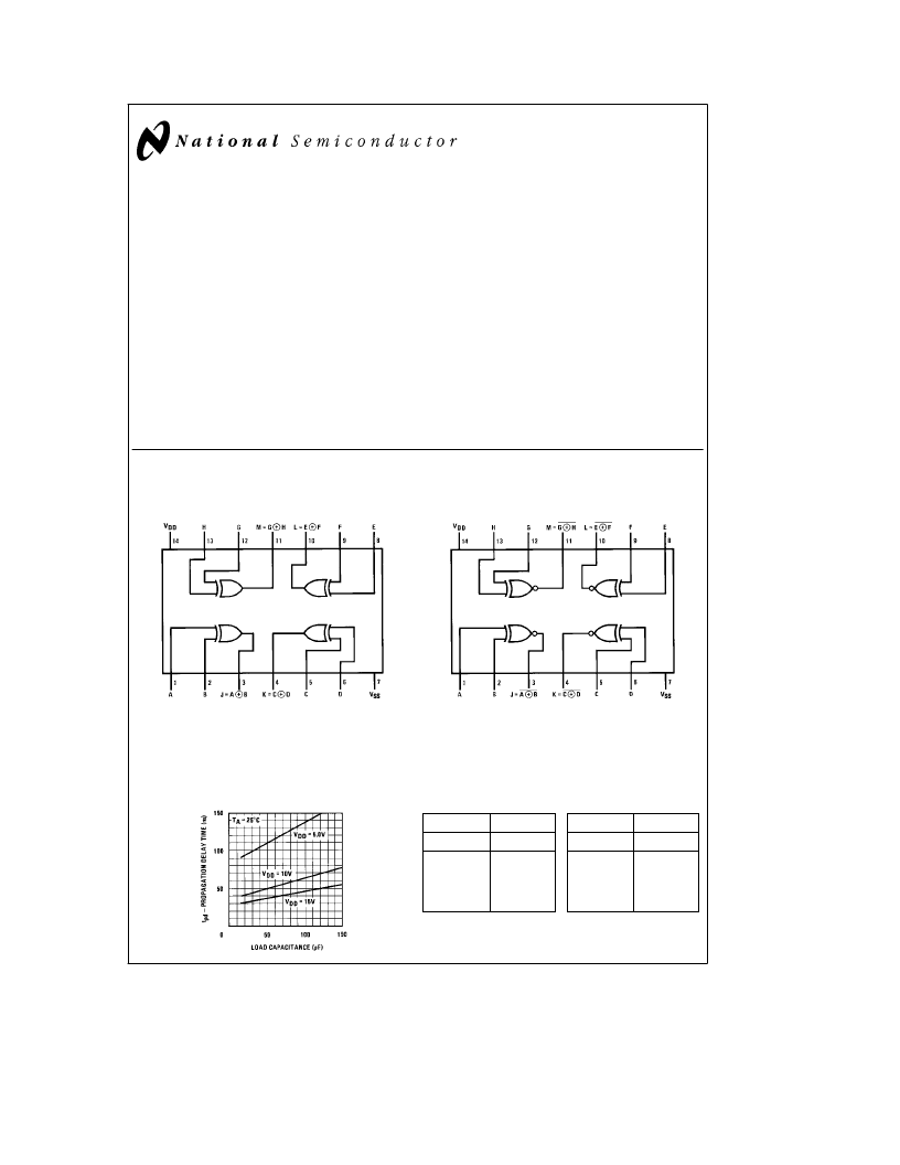
Connection Diagram
CD4070BM/CD4070BC
Dual-In-Line Package
TL/F/5976–1
Top View
CD4077BM/CD4077BC
Dual-In-Line Package
TL/F/5976–5
Top View
Typical Performance
Characteristics
Truth Tables
Propagation Delay Time
vs Load Capacitance
TL/F/5976–2
CD4070BM/CD4070BC
Inputs
Outputs
A
B
Y
L
L
H
H
L
H
L
H
L
H
H
L
CD4077BM/CD4077BC
Inputs
Outputs
A
B
Y
L
L
H
H
L
H
L
H
H
L
L
H
C
1995 National Semiconductor Corporation
RRD-B30M105/Printed in U. S. A.
相關PDF資料 |
PDF描述 |
|---|---|
| QD7-0 | QUADRANT/CIRCULAR DETECTOR |
| QD100-0 | QUADRANT/CIRCULAR DETECTOR |
| QD7-5T | QUADRANT/CIRCULAR DETECTOR |
| QD8224 | CPU System Clock Generator |
| D8224 | CPU System Clock Generator |
相關代理商/技術參數 |
參數描述 |
|---|---|
| QD41242 | 制造商:Panasonic Industrial Company 功能描述:SIDE PANEL |
| QD41465 | 制造商:Panasonic Industrial Company 功能描述:CASE |
| QD4149-REVC | 制造商:Quadrangle 功能描述:POWER CABLE REV B - Bulk |
| QD414PE | 制造商:Eagle Aspen 功能描述:SATELLITE DIEPLEXER5X4 WITH DC HIGH PASS |
| QD4291 REV A | 制造商:Quadrangle 功能描述:HIROSE DF9-31S-1V FLYING LEAD ASSEMBLY - Bulk |
發(fā)布緊急采購,3分鐘左右您將得到回復。