- 您現(xiàn)在的位置:買賣IC網(wǎng) > PDF目錄368396 > PZ3128IS15BE-S Electrically-Erasable Complex PLD PDF資料下載
參數(shù)資料
| 型號: | PZ3128IS15BE-S |
| 英文描述: | Electrically-Erasable Complex PLD |
| 中文描述: | 電可擦除復(fù)雜可編程邏輯器件 |
| 文件頁數(shù): | 11/18頁 |
| 文件大小: | 161K |
| 代理商: | PZ3128IS15BE-S |
R
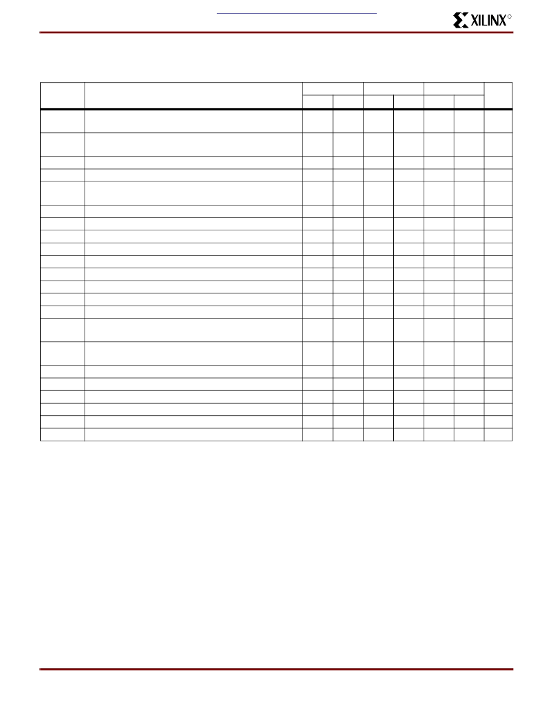
XCR3128: 128 Macrocell CPLD
11
www.xilinx.com
1-800-255-7778
DS034 (v1.3) October 9, 2000
This product has been discontinued. Please see
for details.AC Electrical Characteristics
1
For Commercial Grade Devices
Commercial: 0
°
C
≤
T
AMB
≤
+70
°
C; 3.0V
≤
V
CC
≤
3.6V
Symbol
Parameter
10
12
15
Unit
Min.
2
Max.
10
Min.
2
Max.
12
Min.
2
Max.
15
t
PD_PAL
Propagation delay time, input (or feedback node) to
output through PAL
Propagation delay time, input (or feedback node) to
output through PAL + PLA
Clock to out (global synchronous clock from pin)
Setup time (from input or feedback node) through PAL
Setup time (from input or feedback node) through
PAL + PLA
Hold time
Clock High time
Clock Low time
Input Rise time
Input Fall time
Maximum FF toggle rate
2
1/(t
CH
+ t
CL
)
Maximum internal frequency
2
1/(t
SUPAL
+ t
CF
)
Maximum external frequency
2
1/(t
SUPAL
+ t
CO
)
Output buffer delay time
Input (or feedback node) to internal feedback node delay
time through PAL
Input (or feedback node) to internal feedback node delay
time through PAL+PLA
Clock to internal feedback node delay time
Delay from valid V
DD
to valid reset
Input to output disable
3
Input to output valid
Input to register preset
Input to register reset
ns
t
PD_PLA
3
12.5
3
14.5
3
17.5
ns
t
CO
t
SU_PAL
t
SU_PLA
2
6
7
2
7
8
2
8
9
ns
ns
ns
8.5
9.5
10.5
t
H
t
CH
t
CL
t
R
t
F
f
MAX1
f
MAX2
f
MAX3
t
BUF
t
PDF_PAL
0
0
0
ns
ns
ns
ns
ns
MHz
MHz
MHz
ns
ns
3
3
4
4
4
4
20
20
20
20
20
20
167
87
77
125
74
66
125
65
59
1.5
0.5
1.5
10.5
1.5
13.5
2
2
2
t
PDF_PLA
3
11
3
13
3
16
ns
t
CF
t
INIT
t
ER
t
EA
t
RP
t
RR
Notes:
5.5
50
12.5
12.5
14
14
6.5
50
14
14
16
16
7.5
50
17
17
19
19
ns
μ
s
ns
ns
ns
ns
1. Specifications measured with one output switching. See
Figure 6
and
Table 6
for derating.
2. This parameter guaranteed by design and characterization, not by test.
3. Output C
L
= 5 pF.
相關(guān)PDF資料 |
PDF描述 |
|---|---|
| PZ3128IS15BP | Electrically-Erasable Complex PLD |
| PZ3128IS15BP-S | Electrically-Erasable Complex PLD |
| PZ3128-S10A84 | IC-SM-CMOS PLD |
| PZ3128-S10BB1 | Electrically-Erasable Complex PLD |
| PZ3128-S10BB1-S | Electrically-Erasable Complex PLD |
相關(guān)代理商/技術(shù)參數(shù) |
參數(shù)描述 |
|---|---|
| PZ32146-0120 | 制造商:Foxconn 功能描述: |
| PZ37047-S01-A | 制造商:Foxconn 功能描述:Pga Socket, 370 Contacts, 19x19i, 0.05 Row Spacing, Pc Tail Terminal |
| PZ37047-S01-S | 制造商:Foxconn 功能描述:Pga Socket, 370 Contacts, 19x19i, 0.050 Row Spacing, Pc Tail Terminal |
| PZ3X1-15/16 | 制造商:Eclipse Tools 功能描述: |
| PZ-4-3 | 制造商:RICHARD MANNO 功能描述: |
發(fā)布緊急采購,3分鐘左右您將得到回復(fù)。