- 您現(xiàn)在的位置:買賣IC網(wǎng) > PDF目錄368396 > PZ3128-S10A84 IC-SM-CMOS PLD PDF資料下載
參數(shù)資料
| 型號(hào): | PZ3128-S10A84 |
| 英文描述: | IC-SM-CMOS PLD |
| 中文描述: | 集成電路釤的CMOS可編程邏輯器件 |
| 文件頁(yè)數(shù): | 2/18頁(yè) |
| 文件大小: | 161K |
| 代理商: | PZ3128-S10A84 |
第1頁(yè)當(dāng)前第2頁(yè)第3頁(yè)第4頁(yè)第5頁(yè)第6頁(yè)第7頁(yè)第8頁(yè)第9頁(yè)第10頁(yè)第11頁(yè)第12頁(yè)第13頁(yè)第14頁(yè)第15頁(yè)第16頁(yè)第17頁(yè)第18頁(yè)
R
XCR3128: 128 Macrocell CPLD
DS034 (v1.3) October 9, 2000
www.xilinx.com
1-800-255-7778
2
This product has been discontinued. Please see
for details.The XCR3128 CPLD is electrically reprogrammable using
industry standard device programmers from vendors such
as Data I/O, BP Microsystems, SMS, and others. The
XCR3128 also includes an industry-standard, IEEE 1149.1,
JTAG interface through which in-system programming
(ISP) and reprogramming of the device is supported.
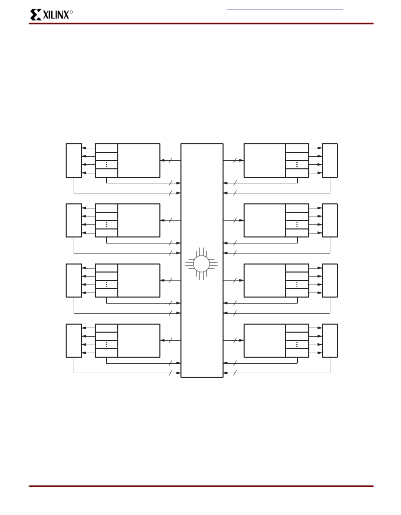
XPLA
Architecture
Figure 1
shows a high level block diagram of a 128 macro-
cell device implementing the XPLA architecture. The XPLA
architecture consists of logic blocks that are interconnected
by a Zero-power Interconnect Array (ZIA). The ZIA is a vir-
tual crosspoint switch. Each logic block is essentially a
36V16 device with 36 inputs from the ZIA and 16 macro-
cells. Each logic block also provides 32 ZIA feedback paths
from the macrocells and I/O pins.
From this point of view, this architecture looks like many
other CPLD architectures. What makes the CoolRunner
family unique is what is inside each logic block and the
design technique used to implement these logic blocks.
The contents of the logic block will be described next.
Figure 1: Xilinx XPLA Architecture
LOGIC
BLOCK
I/O
36
16
16
36
16
16
MC1
MC2
MC16
I/O
MC1
MC2
MC16
LOGIC
BLOCK
I/O
36
16
16
36
16
16
MC1
MC2
MC16
I/O
MC1
MC2
MC16
ZIA
LOGIC
BLOCK
LOGIC
BLOCK
LOGIC
BLOCK
I/O
36
16
16
36
16
16
MC1
MC2
MC16
I/O
MC1
MC2
MC16
LOGIC
BLOCK
LOGIC
BLOCK
I/O
36
16
16
36
16
16
MC1
MC2
MC16
I/O
MC1
MC2
MC16
SP00464
LOGIC
BLOCK
相關(guān)PDF資料 |
PDF描述 |
|---|---|
| PZ3128-S10BB1 | Electrically-Erasable Complex PLD |
| PZ3128-S10BB1-S | Electrically-Erasable Complex PLD |
| PZ3128-S10BB2 | Electrically-Erasable Complex PLD |
| PZ3128-S10BE | Electrically-Erasable Complex PLD |
| PZ3128-S10BE-S | Electrically-Erasable Complex PLD |
相關(guān)代理商/技術(shù)參數(shù) |
參數(shù)描述 |
|---|---|
| PZ32146-0120 | 制造商:Foxconn 功能描述: |
| PZ37047-S01-A | 制造商:Foxconn 功能描述:Pga Socket, 370 Contacts, 19x19i, 0.05 Row Spacing, Pc Tail Terminal |
| PZ37047-S01-S | 制造商:Foxconn 功能描述:Pga Socket, 370 Contacts, 19x19i, 0.050 Row Spacing, Pc Tail Terminal |
| PZ3X1-15/16 | 制造商:Eclipse Tools 功能描述: |
| PZ-4-3 | 制造商:RICHARD MANNO 功能描述: |
發(fā)布緊急采購(gòu),3分鐘左右您將得到回復(fù)。