- 您現(xiàn)在的位置:買賣IC網(wǎng) > PDF目錄69255 > PTH12060WAST (TEXAS INSTRUMENTS INC) 1-OUTPUT DC-DC REG PWR SUPPLY MODULE PDF資料下載
參數(shù)資料
| 型號(hào): | PTH12060WAST |
| 廠商: | TEXAS INSTRUMENTS INC |
| 元件分類: | 電源模塊 |
| 英文描述: | 1-OUTPUT DC-DC REG PWR SUPPLY MODULE |
| 封裝: | DIP-10 |
| 文件頁數(shù): | 15/29頁 |
| 文件大小: | 1040K |
| 代理商: | PTH12060WAST |
第1頁第2頁第3頁第4頁第5頁第6頁第7頁第8頁第9頁第10頁第11頁第12頁第13頁第14頁當(dāng)前第15頁第16頁第17頁第18頁第19頁第20頁第21頁第22頁第23頁第24頁第25頁第26頁第27頁第28頁第29頁
Margin Up/Down Controls
U
D
499
R
99.8 k
%
499
R
99.8 k
%
=
-
W
÷
D
è
=
-
W
÷
D
è
(2)
SLTS217H – MAY 2003 – REVISED DECEMBER 2008 .................................................................................................................................................... www.ti.com
The PTH12060, PTH12010, PTH12020, and PTH12030 products incorporate Margin Up and Margin Down
control inputs. These controls allow the output voltage to be momentarily adjusted [1], either up or down, by a
nominal 5%. This provides a convenient method for dynamically testing the operation of the load circuit over its
supply margin or range. It can also be used to verify the function of supply voltage supervisors. The ±5% change
is applied to the adjusted output voltage, as set by the external resistor, RSET at the VO Adjust pin.
The 5% adjustment is made by pulling the appropriate margin control input directly to the GND terminal [2]. A
low-leakage, open-drain device, such as an n-channel MOSFET or p-channel JFET is recommended for this
purpose [3]. Adjustments of less than 5% can also be accommodated by adding series resistors to the control
inputs. The value of the resistor can be selected from Table 6, or calculated using Equation 2.
Margin Up/Down Adjust Resistance Calculation
To reduce the margin adjustment to a value less than 5%, series resistors are required (See RD and RU in
Equation 2). For the same amount of adjustment, the resistor value calculated for RU and RD is the same. The
formula is as follows.
Where
Δ% = The desired amount of margin adjust in percent.
Notes:
1. The Margin Up and Margin Down controls were not intended to be activated simultaneously. If they are
activated simultaneously, the affect on the output voltage may not completely cancel, resulting in the
possibility of a slightly higher error in the output voltage set point.
2. The ground reference should be a direct connection to the module GND. This produces a more accurate
adjustment at the load circuit terminals. The transistors Q1 and Q2 should be located close to the regulator.
3. The Margin Up and Margin Down control inputs are not compatible with devices that source voltage. This
includes TTL logic. These are analog inputs and should only be controlled with a true open-drain device
(preferably a discrete MOSFET transistor). The device selected should have low off-state leakage current.
Each input sources 8 A when grounded, and has an open-circuit voltage of 0.8 V.
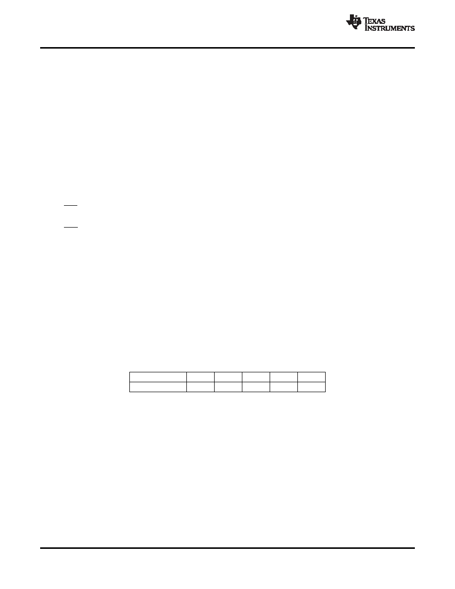
Table 6. Margin Up/Down Resistor Values
% Adjust
5%
4%
3%
2%
1%
RU / RD(k)
0.0
24.9
66.5
150.0
397.0
22
Copyright 2003–2008, Texas Instruments Incorporated
Product Folder Link(s): PTH12060W/L
相關(guān)PDF資料 |
PDF描述 |
|---|---|
| PTH12060WAS | 1-OUTPUT DC-DC REG PWR SUPPLY MODULE |
| PTH12060WAH | 1-OUTPUT DC-DC REG PWR SUPPLY MODULE |
| PTH12060LAZT | 1-OUTPUT DC-DC REG PWR SUPPLY MODULE |
| PTH12060YAS | 1-OUTPUT DC-DC REG PWR SUPPLY MODULE |
| PTH03060YAZT | 1-OUTPUT DC-DC REG PWR SUPPLY MODULE |
相關(guān)代理商/技術(shù)參數(shù) |
參數(shù)描述 |
|---|---|
| PTH12060WAZ | 功能描述:DC/DC轉(zhuǎn)換器 10.8-13.2Vin 5.5V10A 0.995" x0.620"x0.354 RoHS:否 制造商:Murata 產(chǎn)品: 輸出功率: 輸入電壓范圍:3.6 V to 5.5 V 輸入電壓(標(biāo)稱): 輸出端數(shù)量:1 輸出電壓(通道 1):3.3 V 輸出電流(通道 1):600 mA 輸出電壓(通道 2): 輸出電流(通道 2): 安裝風(fēng)格:SMD/SMT 封裝 / 箱體尺寸: |
| PTH12060WAZT | 功能描述:DC/DC轉(zhuǎn)換器 1.2 to 5.5V 10A 12V Input WideAdj Module RoHS:否 制造商:Murata 產(chǎn)品: 輸出功率: 輸入電壓范圍:3.6 V to 5.5 V 輸入電壓(標(biāo)稱): 輸出端數(shù)量:1 輸出電壓(通道 1):3.3 V 輸出電流(通道 1):600 mA 輸出電壓(通道 2): 輸出電流(通道 2): 安裝風(fēng)格:SMD/SMT 封裝 / 箱體尺寸: |
| PTH12060WAZTREP | 制造商:Emerson Network Power - Embedded Power 功能描述: |
| PTH12060WBH | 制造商:Texas Instruments 功能描述: |
| PTH12060Y | 制造商:EMERSON-NETWORKPOWER 制造商全稱:Emerson Network Power 功能描述:Non-isolated DDR/QDR Memory Bus Termination Module |
發(fā)布緊急采購,3分鐘左右您將得到回復(fù)。