- 您現(xiàn)在的位置:買賣IC網(wǎng) > PDF目錄368349 > PT7A4410LJ (Electronic Theatre Controls, Inc.) T1/E1/OC3 System Synchronizer PDF資料下載
參數(shù)資料
| 型號: | PT7A4410LJ |
| 廠商: | Electronic Theatre Controls, Inc. |
| 英文描述: | T1/E1/OC3 System Synchronizer |
| 中文描述: | T1/E1/OC3系統(tǒng)同步 |
| 文件頁數(shù): | 8/34頁 |
| 文件大?。?/td> | 294K |
| 代理商: | PT7A4410LJ |
第1頁第2頁第3頁第4頁第5頁第6頁第7頁當前第8頁第9頁第10頁第11頁第12頁第13頁第14頁第15頁第16頁第17頁第18頁第19頁第20頁第21頁第22頁第23頁第24頁第25頁第26頁第27頁第28頁第29頁第30頁第31頁第32頁第33頁第34頁
||||||||||||||||||||||||||||||||||||||||||||||||||||||||||||||||||||||||||||||||||||||||||||||||||||||||||||||||||||||||||||||||||||||||||||||||||||||||||||||||||||||||||||||||||||||||||||||||||||||||||||||||||||||||||||||||||||||||||||||||||||||||||||||||||||
Data Sheet
PT7A4410/4410L
T1/E1/OC3 System Synchronizer
PT0106(09/02)
Ver:0
8
Whenever there is a change in the input reference source, such
as a switch from the primary reference signal (PRI) to second-
ary reference signal (SEC), the typical result is a step change in
phase of the DPLL input signal that causes an unacceptable
step change in the DPLL input signal phase. The TIE Correc-
tor circuit is used to eliminate the step change in the DPLL
input signal phase, thus maintaining continuity of phase at
the DPLL output.
Referring to Figure 3, the selected reference signal (e.g. SEC)
feeds the Comparing Circuit where it is compared with the
feedback signal from the output circuit. Whenever there is a
step change in the reference input signal
’
s phase, the Compar-
ing Circuit will generates a Delay Value for the Programmable
Delay Circuit. The Delay Circuit then delays the input refer-
ence signal by the Delay Value, thus providing the DPLL with
a Virtual Reference Signal having no phase discontinuity.
The DPLL phase detects and tracks the Virtual Reference Sig-
nal. As the Virtual Reference Signal exhibits no discontinuity
of phase, there is no phase transient in the DPLL output signal.
This is the Normal operation of the device
.
During the input reference signals source switching process, a
holdover state will occurr before the DPLL begins to track the
Virtual Reference Signal. When the input reference is switched
to the new source, the State Machine initiates Holdover State,
during which the DPLL does not use the Virtual Reference
Signal. Instead, it uses stored information to produce a clock
signal that is compared in the Comparing Circuit with the
Feedback Signal. This compared result is sent to the Program-
mable Delay Circuit which in turn delivers to the DPLL input
a new Virtual Reference Signal whose phase is aligned with
that of the previous input reference signal. The State Machine
then terminates Holdover State and return the device to Nor-
mal state.
As the Programmable Delay Circuit maintains the phase of the
Virtual Reference Signal while the TIE Corrector is enabled,
there will in general be a time delay between the chip output
signals and the selected input reference signal after switching
to a new input reference source (e.g. from PRI to SEC). Each
time a new reference source is selected, there will in general be
a new time delay. The value of this delay represents the accu-
mulation of the phase errors measured and corrected for during
the various reference source switching events.
The Programmable Delay Circuit can be zeroed through the
TCLR pin (low level, min. duration 300ns), realigning the
output signals with the present input reference signal. The
speed of realignments is limited by the Limiter in the DPLL to
5ns per 125
μ
s. Convergence is in the direction of least phase
travel.
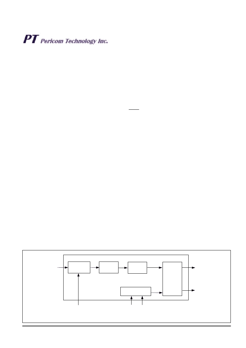
Digital Phase-Locked Loop (DPLL)
The DPLL consists of the Phase Detector, Limiter, Loop Filter,
Digitally Controlled Oscillator (DCO) and Control Circuit.
See Figure 4 for the block diagram of DPLL.
The Virtual Reference Signal from TIE is sent to Phase Detec-
tor for comparison with the Feedback Signal from the Feed-
back Frequency Select MUX. An error signal corresponding to
their instantaneous phase difference is produced and sent to
the Limiter.
The Limiter amplifies this error signal to ensure the DPLL
responds to all input transient conditions with a maximum
output phase slope of 5ns per 125
μ
s. This performance easily
meets the maximum phase slope of 7.6ns per 125
μ
s or 81ns per
1.326ms specified by AT&T TR62411.
The Loop Filter is a 1.9Hz low pass filter for all three reference
frequency selections: 8kHz, 1.544MHz and 2.048MHz. The
filter ensures that the jitter transfer requirements in ETS 300-
011 and AT&T TR62411 are met.
Figure 4. Block Diagram of DPLL
Control Circuit
Phase
Detector
Limiter
Loop
Filter
Virtual
Reference
from TIE
Corrector
Feedback Signal
From
Frequency Select MUX
State Select From
Input Impairment
Monitor
State Select
From
State Machine
DPLL Reference
to
Output Interface
Circuit
DCO
相關PDF資料 |
PDF描述 |
|---|---|
| PT7A8980 | 100V Quad N-Channel HEXFET Power MOSFET in a Power MLP package |
| PT7C4337 | Real-time Clock Module (I2C Bus) |
| PT7C4337PE | Real-time Clock Module (I2C Bus) |
| PT7C4337UE | Real-time Clock Module (I2C Bus) |
| PT7C4337WE | Real-time Clock Module (I2C Bus) |
相關代理商/技術參數(shù) |
參數(shù)描述 |
|---|---|
| PT7A5020 | 制造商:未知廠家 制造商全稱:未知廠家 功能描述:2048 Ports Non-Blocking Time-Slot Switch? |
| PT7A6525 | 制造商:未知廠家 制造商全稱:未知廠家 功能描述:Dual-channel Protocol Controller? | User's manual for PT7A6525(6) demo system in DMA mode?(PDF) |
| PT7A6525L | 制造商:未知廠家 制造商全稱:未知廠家 功能描述:Dual-channel Protocol Controller? | Brief?(PDF) |
| PT7A6526 | 制造商:未知廠家 制造商全稱:未知廠家 功能描述:Single-channel Protocol Controller? | User's manual for PT7A6525(6) demo system in interrupt mode?(PDF) |
| PT7A6527 | 制造商:未知廠家 制造商全稱:未知廠家 功能描述:Quad-channel Protocol Controller? | Demo board Schematic and Program?(PDF) |
發(fā)布緊急采購,3分鐘左右您將得到回復。