- 您現(xiàn)在的位置:買賣IC網(wǎng) > PDF目錄368348 > PT7761N Intelligent Power Switch 1 Channel High Side Driver in a D2-Pak 5-Lead Package PDF資料下載
參數(shù)資料
| 型號: | PT7761N |
| 英文描述: | Intelligent Power Switch 1 Channel High Side Driver in a D2-Pak 5-Lead Package |
| 中文描述: | 模擬IC |
| 文件頁數(shù): | 4/8頁 |
| 文件大?。?/td> | 165K |
| 代理商: | PT7761N |
For technical support and more information, see inside back cover or visit www.ti.com
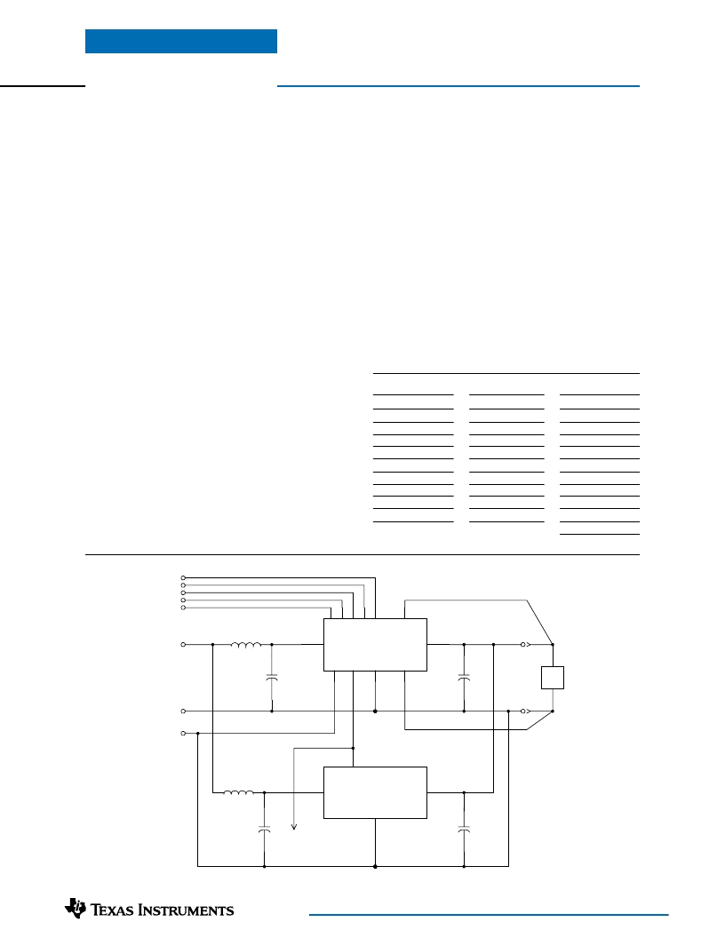
Application Notes
Increasing the PT7761 Output Current with
the PT7769 Compatible Current Booster
The PT7769 is a 40-A “Current Booster” module
for the PT7761 regulator. The booster is controlled
directly by the regulator, and effectively adds a
parallel output stage. This allows the system to run
sychronously, providing a low noise solution. Up to
three booster modules can be connected to a single
regulator. Each booster increases the available output
current by 40A. Combinations of a regulator and
booster modules can supply power for virtually any
multi-processor application.
A current booster is not a stand-alone product, and
can only operate with a regulator. It is housed in
the same package as its compatible regulator, and
shares the same mechanical outline. Except for an
increase in output current, the overall performance
of a PT7761/booster combination is identical to
that of a stand-alone regulator. Refer to the appro-
priate data sheet for the performance specifications.
PT7761, PT7769
Current Booster Application Schematic
C
IN
+
C
OUT
+
LOAD
V
IN
VID0
VID1
VID2
VID3
VID4
V
OUT
GND
GND
STBY*
L
IN
1μH
REMOTE SENSE (
–
)
REMOTE SENSE (+)
PROGRAMMING PINS
C
IN
+
L
IN
1μH
C
OUT
+
PT7761
4
3
2
1
31
23
–
30
15
6
16
–
22
9
–
14
5
7
Sync
GND
Sns (+)
Sns (
–
)
V
OUT
V
IN
Stby
VID0 - VID4
PT7769
7
23
–
30
16
–
22
9
–
14
Synch
V
OUT
GND
V
OUT
To
Additional
Boosters
Table 1; PT7769 Pin-Out Information
Pin Function
1
No Connect
2
No Connect
3
No Connect
4
No Connect
5
No Connect
6
No Connect
7
Sync
8
No Connect
9
V
in
10 V
in
Pin Function
11 V
in
12 V
in
13 V
in
14 V
in
15 No Connect
16 GND
17 GND
18 GND
19 GND
20 GND
Pin Function
21
GND
22
GND
23
V
out
24
V
out
25
V
out
26
V
out
27
V
out
28
V
out
29
V
out
30
V
out
31
No Connect
Notes:
1. Each booster requires the same amount of input and
output capacitance as recommended for a stand-alone
regulator. See the Standard Application schematic and
the respective input/output filter notes in the PT7761
product data sheet. Recommendations on specific
capacitor types are also detailed in the application note,
“Capacitor Recommendations for the PT7761
Integrated Switching Regulator.”
2. The 1-μH filter choke located at the input of each
regulator and booster module (L
in
) is optional for most
applications. If specified, each inductor must be sized
to handle 30ADC at full output load.
3. The pin-out of the current booster modules include a
number pins identified, “No Connect” (see Table 1).
These pins are not connected internally to the module
but must be soldered to a pad to preserve the unit’s
mechanical integrity.
4. A similar PCB footprint and trace layout between the
regulator and each booster will facilitate current sharing
between all modules.
相關(guān)PDF資料 |
PDF描述 |
|---|---|
| PT7769 | Intelligent Power Switch 1 Channel High Side Driver in a TO-220FL Package |
| PT7772A | SMPS Controller |
| PT7772C | SMPS Controller |
| PT7772N | SMPS Controller |
| PT7773 | 0.8V to 3.1V 32 Amp High-Performance Programmable ISR |
相關(guān)代理商/技術(shù)參數(shù) |
參數(shù)描述 |
|---|---|
| PT7769 | 制造商:未知廠家 制造商全稱:未知廠家 功能描述:40A 'Current Booster' for the PT7761 ISR |
| PT7769N | 功能描述:DC/DC轉(zhuǎn)換器 40A Current Booster for the PT7761 ISR RoHS:否 制造商:Murata 產(chǎn)品: 輸出功率: 輸入電壓范圍:3.6 V to 5.5 V 輸入電壓(標(biāo)稱): 輸出端數(shù)量:1 輸出電壓(通道 1):3.3 V 輸出電流(通道 1):600 mA 輸出電壓(通道 2): 輸出電流(通道 2): 安裝風(fēng)格:SMD/SMT 封裝 / 箱體尺寸: |
| PT7770 | 制造商:TI 制造商全稱:Texas Instruments 功能描述:32 AMP HIGH-PERFORMANCE “SLEDGE HAMMER” PROGRAMMABLE ISR |
| PT7771 | 制造商:TI 制造商全稱:Texas Instruments 功能描述:32 AMP HIGH-PERFORMANCE “SLEDGE HAMMER” PROGRAMMABLE ISR |
| PT77715 | 制造商:Texas Instruments 功能描述:ELECTRONIC COMPONENT |
發(fā)布緊急采購,3分鐘左右您將得到回復(fù)。