- 您現(xiàn)在的位置:買賣IC網(wǎng) > PDF目錄69173 > PT5806N (TEXAS INSTRUMENTS INC) 18 A SWITCHING REGULATOR, 350 kHz SWITCHING FREQ-MAX, SMA18 PDF資料下載
參數(shù)資料
| 型號: | PT5806N |
| 廠商: | TEXAS INSTRUMENTS INC |
| 元件分類: | 穩(wěn)壓器 |
| 英文描述: | 18 A SWITCHING REGULATOR, 350 kHz SWITCHING FREQ-MAX, SMA18 |
| 封裝: | ROHS COMPLIANT, SIP-18 |
| 文件頁數(shù): | 2/13頁 |
| 文件大小: | 217K |
| 代理商: | PT5806N |
Application Notes
For technical support and more information, see inside back cover or visit www.ti.com
Using the Margin Up/Down Controls on the
PT5800 & PT5810 Regulator Series
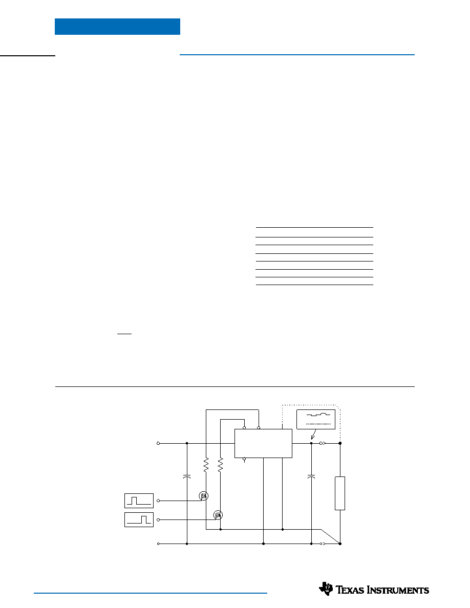
The PT5800 & PT5810 series of integrated switching
regulator modules incorporate Margin Up* (pin 4) and
Margin Dn* (pin 3) control inputs. These controls allow the
output voltage set point to be momentarily adjusted 1,
either up or down, by a nominal 5%. This provides a
convenient method for dynamically testing the load
circuit’s power supply voltage over its operating margin
or range. Note that the ±5% change is also applied to any
adjustment of the output voltage, if made, using the Vo
Adjust (pin 1).
The 5% adjustment is made by driving the appropriate
margin control input directly to the ground reference at
Sense(-) (pin 8) 2. An low-leakage open-drain device, such as
a MOSFET or a p-channel JFET is recommended for this
purpose. Adjustments of less than 5% can also be accom-
modated by adding series resistors to the control inputs
(See Figure 6-1). The value of the resistor can be selected
from Table 6-1, or calculated using the following formula.
Resistor Value Calculation
To reduce the margin adjustment to something less than
5%, series padding resistors are required (See RD and
RU in Figure 6-1). For the same amount of adjustment,
the resistor value calculated for RU and RD will be the
same. The formulas is as follows.
RU/RD =
499
– 99.8
k
%
Where
% = The desired amount of margin adjust in
percent.
Notes:
1. The Margin Up* and Margin Dn* controls were not
intended to be activated simultaneously. If they are
their affects on the output voltage may not completely
cancel, resulting in a slight shift in the output voltage
set point.
2. When possible use the Sense(-) (pin 8) as the ground
reference. This will produce a more accurate adjustment
of the output voltage at the load circuit terminals. GND
(pins 9-13) can be used if the Sense(-) pin is connected
to GND near the regulator.
C
out
+
C
in
+5V
GND
MargDn
L
O
A
D
Q
2
Sense(–)
+V
OUT
GND
PT5800
18
14–17
8
29–13
5, 6, 7
V
OUT
V
IN
GND
SNS(+)
SNS(–)
INHIBIT*
Q
1
4
3
MARG
DN*
MARG
UP*
+
MargUp
0V
+V
o
R
D
R
U
0V
Figure 6-1; Margin Up/Down Application Schematic
Table 6-1; Margin Up/Down Resistor Values
PADDING RESISTOR VALUES
% Adjust
RU / RD
5
0.0k
4
24.9k
3
66.5k
2
150.0k
1
397.0k
PT5800 & PT5810 Series
相關(guān)PDF資料 |
PDF描述 |
|---|---|
| PT5804N | 18 A SWITCHING REGULATOR, 350 kHz SWITCHING FREQ-MAX, SMA18 |
| PT5806A | 18 A SWITCHING REGULATOR, 350 kHz SWITCHING FREQ-MAX, SMA18 |
| PT5804A | 18 A SWITCHING REGULATOR, 350 kHz SWITCHING FREQ-MAX, SMA18 |
| PT5806C | 18 A SWITCHING REGULATOR, 350 kHz SWITCHING FREQ-MAX, SMA18 |
| PT5802C | 18 A SWITCHING REGULATOR, 350 kHz SWITCHING FREQ-MAX, SMA18 |
相關(guān)代理商/技術(shù)參數(shù) |
參數(shù)描述 |
|---|---|
| PT580730 | 制造商:MA-COM 制造商全稱:M/A-COM Technology Solutions, Inc. 功能描述:Miniature Relay |
| PT580L24 | 制造商:MA-COM 制造商全稱:M/A-COM Technology Solutions, Inc. 功能描述:Miniature Relay |
| PT580R24 | 制造商:MA-COM 制造商全稱:M/A-COM Technology Solutions, Inc. 功能描述:Miniature Relay |
| PT580T30 | 制造商:MA-COM 制造商全稱:M/A-COM Technology Solutions, Inc. 功能描述:Miniature Relay |
| PT5810 | 制造商:TI 制造商全稱:Texas Instruments 功能描述:20-A 3.3-V Input Adjustable Integrated Switching Regulator |
發(fā)布緊急采購,3分鐘左右您將得到回復(fù)。