- 您現(xiàn)在的位置:買賣IC網(wǎng) > PDF目錄69171 > PT4853C (TEXAS INSTRUMENTS INC) 3-OUTPUT DC-DC REG PWR SUPPLY MODULE PDF資料下載
參數(shù)資料
| 型號: | PT4853C |
| 廠商: | TEXAS INSTRUMENTS INC |
| 元件分類: | 電源模塊 |
| 英文描述: | 3-OUTPUT DC-DC REG PWR SUPPLY MODULE |
| 封裝: | SIP-26/25 |
| 文件頁數(shù): | 2/15頁 |
| 文件大小: | 268K |
| 代理商: | PT4853C |

For technical support and more information, see inside back cover or visit www.ti.com
Application Notes
PT4850 Series
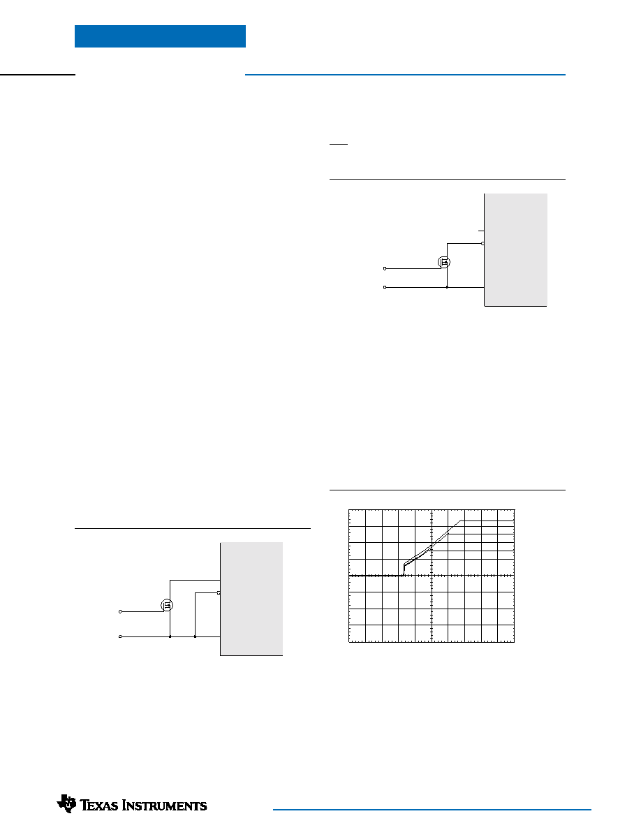
Figure 3; Vo1, Vo2, Vo3 Power-Up Sequence
On/Off Output Voltage Sequencing
The power-up characteristic of the PT4850 series of
DC/DC converters meets the requirements of micro-
processor and DSP chipsets. All three outputs from the
converter are internally sequenced to power up in
unison. Figure 3 shows the waveforms from a PT4851
after power is applied to the input of the converter.
During power-up, all three output voltages rise together
until each reaches their respective output voltage. The
waveforms of Figure 3 were measured with loads of ap-
proximately 50% on each output, with an input source of
48VDC. The converter typically produces a fully regu-
lated output within 150ms.
Using the On/Off Enable Controls on the PT4850
Series of Triple Output DC/DC Converters
The PT4850 (48V input) series of 25-A, triple-output
DC/DC converters incorporate two output enable controls.
EN1 (pin 3) is the Negative Enable input, and EN2 (pin 4)
is the Positive Enable input. Both inputs are electrically
referenced to -Vin (pin 2) on the primary or input side of
the converter. A pull-up resistor is not required, but may
be added if desired. Voltages of up to 70V can be safely
applied to the either of the Enable pins.
Automatic (UVLO) Power-Up
Connecting EN1 (pin 3) to -Vin (pin 2) and leaving EN2
(pin 4) open-circuit configures the converter for auto-
matic power up. (See data sheet “Typical Application”).
The converter control circuitry incorporates an “Under
Voltage Lockout” (UVLO) function, which disables the
converter until the minimum specified input voltage is
present at ±Vin. (See data sheet Specifications). The UVLO
circuitry ensures a clean transition during power-up and
power-down, allowing the converter to tolerate a slow-
rising input voltage. For most applications EN1 and
EN2, can be configured for automatic power-up.
Positive Output Enable (Negative Inhibit)
To configure the converter for a positive enable func-
tion, connect EN1 (pin 3) to -Vin (pin 2), and apply the
system On/Off control signal to EN2 (pin 4). In this
configuration, a low-level input voltage (-Vin potential)
applied to pin 4 disables the converter outputs. Figure 1
is an example of this configuration.
Negative Output Enable (Positive Inhibit)
To configure the converter for a negative enable function,
EN2 (pin 4) is left open circuit, and the system On/Off
control signal is applied to EN1 (pin 3). A low-level
input voltage (-Vin potential) must then be applied to
DC/DC
Module
EN 1*
EN 2
–Vin
–V
IN
1 =Outputs Off
4
3
2
BSS138
DC/DC
Module
EN 1*
EN 2
–Vin
–V
IN
1 =Outputs On
4
3
2
BSS138
Figure 2; Negative Enable Configuration
Figure 1; Positive Enable Configuration
During turn-off, all outputs drop rapidly due to the
discharging effect of actively switched rectifiers. The
voltage at Vo2 remains higher than Vo3 during this
period. The discharge time is typically 100s, but will
vary with the amount of external load capacitance.
pin 3 in order to enable the outputs of the converter.
An example of this configuration is detailed in Figure 2.
Note: The converter will only produce and output voltage if a
valid input voltage is applied to ±Vin.
Vo1 (1V/Div)
V02 (1V/Div)
Vo3 (1V/Div)
HORIZ SCALE: 20ms/Div
相關PDF資料 |
PDF描述 |
|---|---|
| PT4856C | 3-OUTPUT DC-DC REG PWR SUPPLY MODULE |
| PT4854A | 3-OUTPUT DC-DC REG PWR SUPPLY MODULE |
| PT4851C | 3-OUTPUT DC-DC REG PWR SUPPLY MODULE |
| PT4853N | 3-OUTPUT DC-DC REG PWR SUPPLY MODULE |
| PT5021H | 1.5 A SWITCHING REGULATOR, 1200 kHz SWITCHING FREQ-MAX, PSMA3 |
相關代理商/技術參數(shù) |
參數(shù)描述 |
|---|---|
| PT4853N | 功能描述:直流/直流開關轉(zhuǎn)換器 Triple-Output Iso DC-DC Cnvtr RoHS:否 制造商:STMicroelectronics 最大輸入電壓:4.5 V 開關頻率:1.5 MHz 輸出電壓:4.6 V 輸出電流:250 mA 輸出端數(shù)量:2 最大工作溫度:+ 85 C 安裝風格:SMD/SMT |
| PT4854 | 制造商:TI 制造商全稱:Texas Instruments 功能描述:25-A Triple Output Isolated DC/DC Converter For Logic Applications |
| PT4854A | 功能描述:直流/直流開關轉(zhuǎn)換器 Triple-Output Iso DC-DC Cnvtr RoHS:否 制造商:STMicroelectronics 最大輸入電壓:4.5 V 開關頻率:1.5 MHz 輸出電壓:4.6 V 輸出電流:250 mA 輸出端數(shù)量:2 最大工作溫度:+ 85 C 安裝風格:SMD/SMT |
| PT4854C | 功能描述:直流/直流開關轉(zhuǎn)換器 Triple-Output Iso DC-DC Cnvtr RoHS:否 制造商:STMicroelectronics 最大輸入電壓:4.5 V 開關頻率:1.5 MHz 輸出電壓:4.6 V 輸出電流:250 mA 輸出端數(shù)量:2 最大工作溫度:+ 85 C 安裝風格:SMD/SMT |
| PT4854N | 功能描述:DC/DC轉(zhuǎn)換器 Triple-Output Iso DC-DC Cnvtr RoHS:否 制造商:Murata 產(chǎn)品: 輸出功率: 輸入電壓范圍:3.6 V to 5.5 V 輸入電壓(標稱): 輸出端數(shù)量:1 輸出電壓(通道 1):3.3 V 輸出電流(通道 1):600 mA 輸出電壓(通道 2): 輸出電流(通道 2): 安裝風格:SMD/SMT 封裝 / 箱體尺寸: |
發(fā)布緊急采購,3分鐘左右您將得到回復。