- 您現(xiàn)在的位置:買賣IC網(wǎng) > PDF目錄98061 > PT4841A (TEXAS INSTRUMENTS INC) 3-OUTPUT 65 W DC-DC REG PWR SUPPLY MODULE PDF資料下載
參數(shù)資料
| 型號: | PT4841A |
| 廠商: | TEXAS INSTRUMENTS INC |
| 元件分類: | 電源模塊 |
| 英文描述: | 3-OUTPUT 65 W DC-DC REG PWR SUPPLY MODULE |
| 封裝: | SIP-21 |
| 文件頁數(shù): | 8/15頁 |
| 文件大小: | 260K |
| 代理商: | PT4841A |
For technical support and more information, see inside back cover or visit www.ti.com
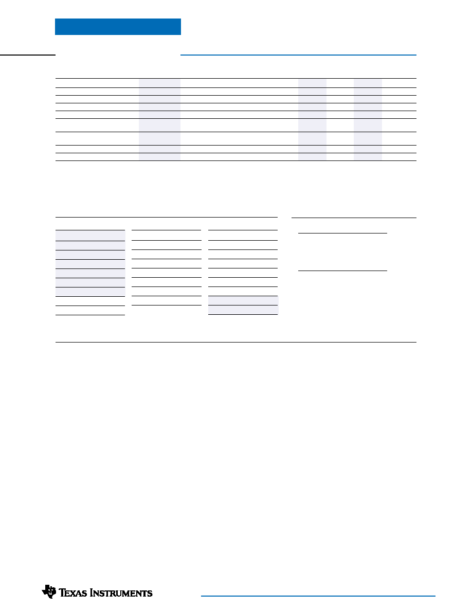
Pin Function
1+Vin
2–Vin
3
EN 1
4
EN 2
5
TEMP
6
Do Not Connect
7
Do Not Connect
8
Pin Not Present
9
Pin Not Present
PT4840 Series—48V
65-W Triple Output Isolated DC/DC
Converter for DSL Applications
Pin Function
10
Pin Not Present
11
+Vo1
12
COM
13
COM
14
Pin Not Present
15+Vo2
16+Vo2
17Vo2 adjust
Pin Function
18
COM
19
COM
20
COM
21Vo3 adjust
22
+Vo3
23
+Vo3
24
Pin Not Present
25
Do Not Connect
26
Do Not Connect
On/Off Enable Logic
Pin Configuration
Pin Descriptions
Pin 3
Pin 4
Output Status
1
×
Off
01On
×
0
Off
Notes:
Logic 1 =Open collector
Logic 0 = –Vin (pin 2) potential
For positive Enable function, connect pin 3
to pin 2 and use pin 4.
For negative Enable function, leave pin 4
open and use pin 3.
+Vin:
The positive input supply for the module with
respect to –Vin. When powering the module from a
–48V telecom central office supply, this input is
connected to the primary system ground.
–Vin:
The negative input supply for the module, and
the 0VDC reference for the EN 1, EN 2, and TEMP
inputs. When powering the module from a +48V
supply, this input is connected to the 48V(Return).
EN 1:
The negative logic input that activates the
module output. This pin is referenced to –Vin. A
low-level voltage at this pin enables the module’s
outputs, and a high impedance impedance disables
the module’s outputs. If not used, the pin must be
connected to –Vin.
EN 2:
The positive logic input that activates the
module output. This pin is referenced to –Vin. A
high impedance at this pin enables the module’s
outputs. If not used, the pin should be left open
circuit.
TEMP:
This pin produces an output signal that tracks
a temperature that is approximately the module’s
metal case. The output voltage is referenced to –Vin
and rises approximately 10mV/°C from an intital
value of 0.1VDC at –40°C. The signal is available
whenever the module is supplied with a valid input
voltage, and is independant of the enable logic status.
(Note: A load impedance of less than 1M
will adversly
affect the module’s over-temperature shutdown threshold.
Use a high-impedance input when monitoring this signal.)
Vo 1:
The highest regulated output voltage, which is
referenced to the COM node. The output may be
used to power analog support circuitry.
Vo 2:
The regulated output that is designed to power
logic or I/O circuitry. It is referenced to the COM
node.
Vo 3:
The low-voltage regulated output that provides
power for a micro, processor, ASIC, or DSP core,
and is referenced to the COM node.
COM:
The secondary return reference for the module’s
three regulated output voltages. It is DC isolated from
the input supply pins.
Vo2 Adjust: Using a single resistor, this pin allows Vo2
to be adjusted higher or lower than the preset value.
If not used, this pin should be left open circuit.
Vo3 Adjust: Using a single resistor, this pin allows Vo3
to be adjusted higher or lower than the preset value.
If not used, this pin should be left open circuit.
Note: Shaded functions indicate those pins that are at primary-side potential.
SLTS142C - DECEMBER 2000 -REVISED SEPTEMBER 2002
Environmental Specifications
Characteristics
Symbols
Conditions
Min
Typ
Max
Units
Operating Temperature Range
Ta
Over Vin Range
–40
—
85 (i)
°C
Over-Temperature Protection
OTP
Case temperature
100
—
°C
Solder Reflow Temperature
Treflow
Surface temperature of module pins or case
—
215 (ii)
°C
Storage Temperature
Ts
—
–40
—
125
°C
Mechanical Shock
Per Mil-STD-883D, Method 2002.3
1 msec, Sine, mounted
—
500
—
G’s
Mechanical Vibration
Mil-STD-883D Method 2007.2
Suffix N
—
10 (iii)
—
G’s
20-2000 Hz
Suffix A, C
—
20 (iii)
—
Weight
—
Vertical/Horizontal
—
90
—
grams
Flammability
—
Meets UL 94V-O
Notes:
(i) See SOA curves or consult factory for appropriate derating.
(ii) During solder reflow of SMD package version do not elevate the module case, pins, or internal component temperatures above a peak of 215°C. For
further guidance refer to the application note, “Reflow Soldering Requirements for Plug-in Power Surface Mount Products,” (SLTA051).
(iii) Only the case pins on through-hole pin configurations (N & A) must be soldered. For more information see the applicable package outline drawing.
相關(guān)PDF資料 |
PDF描述 |
|---|---|
| PT4842A | 3-OUTPUT 62 W DC-DC REG PWR SUPPLY MODULE |
| PT5102S | 2.6 A SWITCHING REGULATOR, 800 kHz SWITCHING FREQ-MAX, SMA3 |
| PT5103J | 2.6 A SWITCHING REGULATOR, 875 kHz SWITCHING FREQ-MAX, SMA3 |
| PT5103H | 2.6 A SWITCHING REGULATOR, 875 kHz SWITCHING FREQ-MAX, SMA3 |
| PT5105L | 2.6 A SWITCHING REGULATOR, 800 kHz SWITCHING FREQ-MAX, SMA3 |
相關(guān)代理商/技術(shù)參數(shù) |
參數(shù)描述 |
|---|---|
| PT4841C | 制造商:未知廠家 制造商全稱:未知廠家 功能描述:DC to DC Converter |
| PT4841N | 制造商:未知廠家 制造商全稱:未知廠家 功能描述:DC to DC Converter |
| PT4842 | 制造商:未知廠家 制造商全稱:未知廠家 功能描述:12V/3.3V/1.8V 48V-Input 62-Watt Triple-Output DC/DC Converter |
| PT4842A | 功能描述:直流/直流開關(guān)轉(zhuǎn)換器 12/3.3/1.8V 48V-Inp 62W 3-Out DC-DC RoHS:否 制造商:STMicroelectronics 最大輸入電壓:4.5 V 開關(guān)頻率:1.5 MHz 輸出電壓:4.6 V 輸出電流:250 mA 輸出端數(shù)量:2 最大工作溫度:+ 85 C 安裝風格:SMD/SMT |
| PT4842C | 功能描述:直流/直流開關(guān)轉(zhuǎn)換器 12/3.3/1.8V 48V-Inp 62W 3-Out DC-DC RoHS:否 制造商:STMicroelectronics 最大輸入電壓:4.5 V 開關(guān)頻率:1.5 MHz 輸出電壓:4.6 V 輸出電流:250 mA 輸出端數(shù)量:2 最大工作溫度:+ 85 C 安裝風格:SMD/SMT |
發(fā)布緊急采購,3分鐘左右您將得到回復(fù)。