- 您現(xiàn)在的位置:買賣IC網(wǎng) > PDF目錄368272 > PSD935F2V-90U (意法半導(dǎo)體) Configurable Memory System on a Chip for 8-Bit Microcontrollers PDF資料下載
參數(shù)資料
| 型號: | PSD935F2V-90U |
| 廠商: | 意法半導(dǎo)體 |
| 英文描述: | Configurable Memory System on a Chip for 8-Bit Microcontrollers |
| 中文描述: | 在8片位微控制器可配置存儲系統(tǒng) |
| 文件頁數(shù): | 55/91頁 |
| 文件大小: | 488K |
| 代理商: | PSD935F2V-90U |
第1頁第2頁第3頁第4頁第5頁第6頁第7頁第8頁第9頁第10頁第11頁第12頁第13頁第14頁第15頁第16頁第17頁第18頁第19頁第20頁第21頁第22頁第23頁第24頁第25頁第26頁第27頁第28頁第29頁第30頁第31頁第32頁第33頁第34頁第35頁第36頁第37頁第38頁第39頁第40頁第41頁第42頁第43頁第44頁第45頁第46頁第47頁第48頁第49頁第50頁第51頁第52頁第53頁第54頁當(dāng)前第55頁第56頁第57頁第58頁第59頁第60頁第61頁第62頁第63頁第64頁第65頁第66頁第67頁第68頁第69頁第70頁第71頁第72頁第73頁第74頁第75頁第76頁第77頁第78頁第79頁第80頁第81頁第82頁第83頁第84頁第85頁第86頁第87頁第88頁第89頁第90頁第91頁
PSD9XX Family
PSD935G2
54
The
PSD935G2
Functional
Blocks
(cont.)
I
DATA OUT
REG.
D
Q
D
G
Q
D
Q
D
Q
WR
WR
WR
ADDRESS
ALE
READ MUX
P
D
B
CONTROL REG.
DIR REG.
PLD INPUT (PORT F)
ISP OR BATTERY BACK-UP (PORT E)
DATA IN
OUTPUT
SELECT
OUTPUT
MUX
PORT PIN
DATA OUT
ADDRESS
A[7:0] OR A[15:8]
CONFIGURATION
BIT
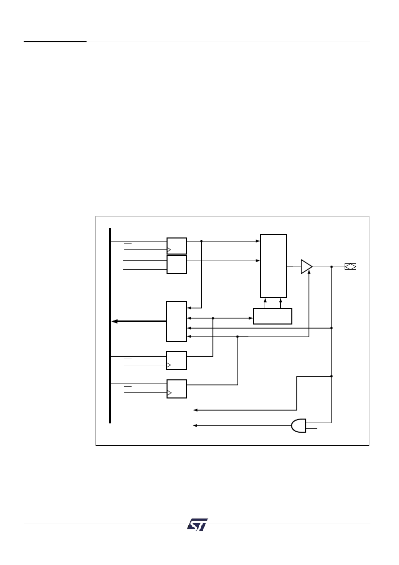
Figure 23. Ports E, F and G Structure
9.4.8 Port F – Functionality and Structure
Port F can be configured to perform one or more of the following functions:
J
MCU I/O Mode
J
PLD Input – as direct input ot the PLD array.
J
Address In – additional high address inputs. Direct input to the PLD array.
J
Latched Address Out – Provide latched address out per Table 18.
J
Slew Rate – pins can be set up for fast slew rate.
J
Data Port – connected to D[7:0] when Port F is configured as Data Port for a
non-multiplexed bus.
9.4.9 Port G – Functionality and Structure
Port G can be configured to perform one or more of the following functions:
J
MCU I/O Mode
J
Latched Address Out – Provide latched address out per Table 18.
J
Open Drain – pins can be configured in Open Drain Mode
發(fā)布緊急采購,3分鐘左右您將得到回復(fù)。