- 您現(xiàn)在的位置:買賣IC網(wǎng) > PDF目錄376278 > PSD9342V20MIT (意法半導(dǎo)體) Flash In-System Programmable ISP Peripherals For 8-bit MCUs PDF資料下載
參數(shù)資料
| 型號: | PSD9342V20MIT |
| 廠商: | 意法半導(dǎo)體 |
| 英文描述: | Flash In-System Programmable ISP Peripherals For 8-bit MCUs |
| 中文描述: | Flash在系統(tǒng)可編程ISP的外設(shè)的8位微控制器 |
| 文件頁數(shù): | 56/110頁 |
| 文件大小: | 1737K |
| 代理商: | PSD9342V20MIT |
第1頁第2頁第3頁第4頁第5頁第6頁第7頁第8頁第9頁第10頁第11頁第12頁第13頁第14頁第15頁第16頁第17頁第18頁第19頁第20頁第21頁第22頁第23頁第24頁第25頁第26頁第27頁第28頁第29頁第30頁第31頁第32頁第33頁第34頁第35頁第36頁第37頁第38頁第39頁第40頁第41頁第42頁第43頁第44頁第45頁第46頁第47頁第48頁第49頁第50頁第51頁第52頁第53頁第54頁第55頁當(dāng)前第56頁第57頁第58頁第59頁第60頁第61頁第62頁第63頁第64頁第65頁第66頁第67頁第68頁第69頁第70頁第71頁第72頁第73頁第74頁第75頁第76頁第77頁第78頁第79頁第80頁第81頁第82頁第83頁第84頁第85頁第86頁第87頁第88頁第89頁第90頁第91頁第92頁第93頁第94頁第95頁第96頁第97頁第98頁第99頁第100頁第101頁第102頁第103頁第104頁第105頁第106頁第107頁第108頁第109頁第110頁
PSD813F2, PSD833F2, PSD834F2, PSD853F2, PSD854F2
56/110
JTAG In-System Programming (ISP)
Port C is JTAG compliant, and can be used for In-
System Programming (ISP). You can multiplex
JTAG operations with other functions on Port C
because In-System Programming (ISP) is not per-
formed in normal Operating mode. For more infor-
mation on the JTAG Port, see the section entitled
PROGRAMMING IN-CIRCUIT USING THE JTAG
SERIAL INTERFACE, page 69
.
Port Configuration Registers (PCR)
Each Port has a set of Port Configuration Regis-
ters (PCR) used for configuration. The contents of
the registers can be accessed by the MCU through
normal READ/WRITE bus cycles at the addresses
given in
Table 7., page 18
. The addresses in Ta-
ble
7
are the offsets in hexadecimal from the base
of the CSIOP register.
The pins of a port are individually configurable and
each bit in the register controls its respective pin.
For example, Bit 0 in a register refers to Bit 0 of its
port. The three Port Configuration Registers
(PCR), shown in Table
22
, are used for setting the
Port configurations. The default Power-up state for
each register in Table
22
is 00h.
Control Register
Any bit reset to '0' in the Control Register sets the
corresponding port pin to MCU I/O Mode, and a '1'
sets it to Address Out Mode. The default mode is
MCU I/O. Only Ports A and B have an associated
Control Register.
Direction Register
The Direction Register, in conjunction with the out-
put enable (except for Port D), controls the direc-
tion of data flow in the I/O Ports. Any bit set to '1'
in the Direction Register causes the correspond-
ing pin to be an output, and any bit set to '0' causes
it to be an input. The default mode for all port pins
is input.
Figure 28., page 58
and
Figure 29., page 59
show
the Port Architecture diagrams for Ports A/B and
C, respectively. The direction of data flow for Ports
A, B, and C are controlled not only by the direction
register, but also by the output enable product
term from the PLD AND Array. If the output enable
product term is not active, the Direction Register
has sole control of a given pin’s direction.
An example of a configuration for a Port with the
three least significant bits set to output and the re-
mainder set to input is shown in Table
25
. Since
Port D only contains three pins (shown in
Figure
31., page 61
), the Direction Register for Port D
has only the three least significant bits active.
Drive Select Register
The Drive Select Register configures the pin driver
as Open Drain or CMOS for some port pins, and
controls the slew rate for the other port pins. An
external pull-up resistor should be used for pins
configured as Open Drain.
A pin can be configured as Open Drain if its corre-
sponding bit in the Drive Select Register is set to a
’1.’ The default pin drive is CMOS.
Note that the slew rate is a measurement of the
rise and fall times of an output. A higher slew rate
means a faster output response and may create
more electrical noise. A pin operates in a high slew
rate when the corresponding bit in the Drive Reg-
ister is set to ’1.’ The default rate is slow slew.
Table 26., page 57
shows the Drive Register for
Ports A, B, C, and D. It summarizes which pins can
be configured as Open Drain outputs and which
pins the slew rate can be set for.
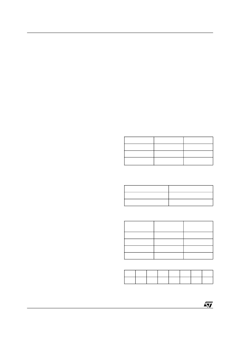
Table 22. Port Configuration Registers (PCR)
Note: 1. See
Table 26., page 57
for Drive Register bit definition.
Table 23. Port Pin Direction Control, Output
Enable P.T. Not Defined
Table 24. Port Pin Direction Control, Output
Enable P.T. Defined
Table 25. Port Direction Assignment Example
Register Name
Port
MCU Access
Control
A,B
WRITE/READ
Direction
A,B,C,D
WRITE/READ
Drive Select
1
A,B,C,D
WRITE/READ
Direction Register Bit
Port Pin Mode
0
Input
1
Output
Direction
Register Bit
Output Enable
P.T.
Port Pin Mode
0
0
Input
0
1
Output
1
0
Output
1
1
Output
Bit 7 Bit 6 Bit 5 Bit 4 Bit 3 Bit 2 Bit 1 Bit 0
0
0
0
0
0
1
1
1
相關(guān)PDF資料 |
PDF描述 |
|---|---|
| PSD9133V20MIT | Flash In-System Programmable ISP Peripherals For 8-bit MCUs |
| PSD8533V20MIT | Flash In-System Programmable ISP Peripherals For 8-bit MCUs |
| PSD9533V20MIT | Flash In-System Programmable ISP Peripherals For 8-bit MCUs |
| PSD8143V20MIT | Flash In-System Programmable ISP Peripherals For 8-bit MCUs |
| PSD9143V20MIT | Flash In-System Programmable ISP Peripherals For 8-bit MCUs |
相關(guān)代理商/技術(shù)參數(shù) |
參數(shù)描述 |
|---|---|
| PSD934F2-15J | 功能描述:SPLD - 簡單可編程邏輯器件 5V 2M 150ns RoHS:否 制造商:Texas Instruments 邏輯系列:TICPAL22V10Z 大電池數(shù)量:10 最大工作頻率:66 MHz 延遲時間:25 ns 工作電源電壓:4.75 V to 5.25 V 電源電流:100 uA 最大工作溫度:+ 75 C 最小工作溫度:0 C 安裝風(fēng)格:Through Hole 封裝 / 箱體:DIP-24 |
| PSD934F290J | 制造商:WSI 功能描述: |
| PSD934F2-90J | 功能描述:SPLD - 簡單可編程邏輯器件 PLCC-52 5V 2M 90NS RoHS:否 制造商:Texas Instruments 邏輯系列:TICPAL22V10Z 大電池數(shù)量:10 最大工作頻率:66 MHz 延遲時間:25 ns 工作電源電壓:4.75 V to 5.25 V 電源電流:100 uA 最大工作溫度:+ 75 C 最小工作溫度:0 C 安裝風(fēng)格:Through Hole 封裝 / 箱體:DIP-24 |
| PSD934F2-90M | 功能描述:SPLD - 簡單可編程邏輯器件 5V 2M 90ns RoHS:否 制造商:Texas Instruments 邏輯系列:TICPAL22V10Z 大電池數(shù)量:10 最大工作頻率:66 MHz 延遲時間:25 ns 工作電源電壓:4.75 V to 5.25 V 電源電流:100 uA 最大工作溫度:+ 75 C 最小工作溫度:0 C 安裝風(fēng)格:Through Hole 封裝 / 箱體:DIP-24 |
| PSD934F2V-15J | 功能描述:SPLD - 簡單可編程邏輯器件 3.3V 2M 150ns RoHS:否 制造商:Texas Instruments 邏輯系列:TICPAL22V10Z 大電池數(shù)量:10 最大工作頻率:66 MHz 延遲時間:25 ns 工作電源電壓:4.75 V to 5.25 V 電源電流:100 uA 最大工作溫度:+ 75 C 最小工作溫度:0 C 安裝風(fēng)格:Through Hole 封裝 / 箱體:DIP-24 |
發(fā)布緊急采購,3分鐘左右您將得到回復(fù)。