- 您現(xiàn)在的位置:買(mǎi)賣(mài)IC網(wǎng) > PDF目錄368264 > PSD835G3V-70U (意法半導(dǎo)體) Configurable Memory System on a Chip for 8-Bit Microcontrollers PDF資料下載
參數(shù)資料
| 型號(hào): | PSD835G3V-70U |
| 廠商: | 意法半導(dǎo)體 |
| 英文描述: | Configurable Memory System on a Chip for 8-Bit Microcontrollers |
| 中文描述: | 在8片位微控制器可配置存儲(chǔ)系統(tǒng) |
| 文件頁(yè)數(shù): | 12/110頁(yè) |
| 文件大?。?/td> | 570K |
| 代理商: | PSD835G3V-70U |
第1頁(yè)第2頁(yè)第3頁(yè)第4頁(yè)第5頁(yè)第6頁(yè)第7頁(yè)第8頁(yè)第9頁(yè)第10頁(yè)第11頁(yè)當(dāng)前第12頁(yè)第13頁(yè)第14頁(yè)第15頁(yè)第16頁(yè)第17頁(yè)第18頁(yè)第19頁(yè)第20頁(yè)第21頁(yè)第22頁(yè)第23頁(yè)第24頁(yè)第25頁(yè)第26頁(yè)第27頁(yè)第28頁(yè)第29頁(yè)第30頁(yè)第31頁(yè)第32頁(yè)第33頁(yè)第34頁(yè)第35頁(yè)第36頁(yè)第37頁(yè)第38頁(yè)第39頁(yè)第40頁(yè)第41頁(yè)第42頁(yè)第43頁(yè)第44頁(yè)第45頁(yè)第46頁(yè)第47頁(yè)第48頁(yè)第49頁(yè)第50頁(yè)第51頁(yè)第52頁(yè)第53頁(yè)第54頁(yè)第55頁(yè)第56頁(yè)第57頁(yè)第58頁(yè)第59頁(yè)第60頁(yè)第61頁(yè)第62頁(yè)第63頁(yè)第64頁(yè)第65頁(yè)第66頁(yè)第67頁(yè)第68頁(yè)第69頁(yè)第70頁(yè)第71頁(yè)第72頁(yè)第73頁(yè)第74頁(yè)第75頁(yè)第76頁(yè)第77頁(yè)第78頁(yè)第79頁(yè)第80頁(yè)第81頁(yè)第82頁(yè)第83頁(yè)第84頁(yè)第85頁(yè)第86頁(yè)第87頁(yè)第88頁(yè)第89頁(yè)第90頁(yè)第91頁(yè)第92頁(yè)第93頁(yè)第94頁(yè)第95頁(yè)第96頁(yè)第97頁(yè)第98頁(yè)第99頁(yè)第100頁(yè)第101頁(yè)第102頁(yè)第103頁(yè)第104頁(yè)第105頁(yè)第106頁(yè)第107頁(yè)第108頁(yè)第109頁(yè)第110頁(yè)
PSD835G2
PSD8XX Family
11
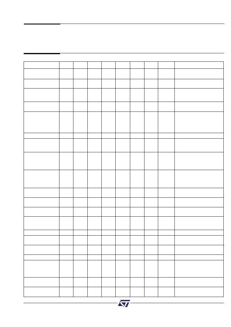
Table 6 shows the offset addresses to the PSD835G2 registers relative to the CSIOP base
address. The CSIOP space is the 256 bytes of address that is allocated by the user to the
internal PSD835G2 registers. Table 6 provides brief descriptions of the registers in CSIOP
space. For a more detailed description, refer to section 9.
7.0 PSD835G2
Register
Description and
Address Offset
Register Name
Port A
Port B
Port C
Port D
Port E
Port F
Port G
Other*
Description
Data In
00
01
10
11
30
40
41
Reads Port pin as input,
MCU I/O input mode
Selects mode between
MCU I/O or Address Out
Stores data for output
to Port pins, MCU I/O
output mode
Configures Port pin as
input or output
Configures Port pins as
either CMOS or Open
Drain on some pins, while
selecting high slew rate
on other pins.
Reads Input Micro
Cells
Reads the status of the
output enable to the I/O
Port driver
Read – reads output of
Micro
Cells A
Write – loads Micro
cell
Flip-Flops
Read – reads output of
Micro
Cells B
Write – loads Micro
cell
Flip-Flops
Blocks writing to the
Output Micro
Cells A
Blocks writing to the
Output Micro
Cells B
Read only – Flash Sector
Protection
Read only – PSD Security
and Flash Boot Sector
Protection
Enables JTAG Port
Power Management
Register 0
Power Management
Register 2
Page Register
Places PSD memory
areas in Program and/or
Data space on an
individual basis.
Read only – Flash and
SRAM size
Read only – Boot type
and size
Control
32
42
43
Data Out
04
05
14
15
34
44
45
Direction
06
07
16
17
36
46
47
Drive Select
08
09
18
19
38
48
49
Input Micro
Cell
0A
0B
1A
Enable Out
0C
0D
1C
4C
Output
Micro
Cells A
20
Output
Micro
Cells B
21
Mask
Micro
Cells A
Mask
Micro
Cells B
22
23
Flash Protection
C0
Flash Boot
Protection
C2
JTAG Enable
C7
PMMR0
B0
PMMR2
B4
Page
E0
VM
E2
Memory_ID0
F0
Memory_ID1
F1
Table 6. Register Address Offset
相關(guān)PDF資料 |
PDF描述 |
|---|---|
| PSD835G3V-70UI | Configurable Memory System on a Chip for 8-Bit Microcontrollers |
| PSD835G3V-90B81 | Configurable Memory System on a Chip for 8-Bit Microcontrollers |
| PSD835G3V-90B81I | Configurable Memory System on a Chip for 8-Bit Microcontrollers |
| PSD835G3V-90J | Configurable Memory System on a Chip for 8-Bit Microcontrollers |
| PSD835G3V-90JI | Configurable Memory System on a Chip for 8-Bit Microcontrollers |
相關(guān)代理商/技術(shù)參數(shù) |
參數(shù)描述 |
|---|---|
| PSD853F2-70J | 功能描述:SPLD - 簡(jiǎn)單可編程邏輯器件 5.0V 1M 70ns RoHS:否 制造商:Texas Instruments 邏輯系列:TICPAL22V10Z 大電池?cái)?shù)量:10 最大工作頻率:66 MHz 延遲時(shí)間:25 ns 工作電源電壓:4.75 V to 5.25 V 電源電流:100 uA 最大工作溫度:+ 75 C 最小工作溫度:0 C 安裝風(fēng)格:Through Hole 封裝 / 箱體:DIP-24 |
| PSD853F2-70M | 功能描述:CPLD - 復(fù)雜可編程邏輯器件 5.0V 1M 70ns RoHS:否 制造商:Lattice 系列: 存儲(chǔ)類(lèi)型:EEPROM 大電池?cái)?shù)量:128 最大工作頻率:333 MHz 延遲時(shí)間:2.7 ns 可編程輸入/輸出端數(shù)量:64 工作電源電壓:3.3 V 最大工作溫度:+ 90 C 最小工作溫度:0 C 封裝 / 箱體:TQFP-100 |
| PSD853F2-90J | 功能描述:CPLD - 復(fù)雜可編程邏輯器件 5.0V 1M 90ns RoHS:否 制造商:Lattice 系列: 存儲(chǔ)類(lèi)型:EEPROM 大電池?cái)?shù)量:128 最大工作頻率:333 MHz 延遲時(shí)間:2.7 ns 可編程輸入/輸出端數(shù)量:64 工作電源電壓:3.3 V 最大工作溫度:+ 90 C 最小工作溫度:0 C 封裝 / 箱體:TQFP-100 |
| PSD853F2-90JI | 功能描述:CPLD - 復(fù)雜可編程邏輯器件 5.0V 1M 90ns RoHS:否 制造商:Lattice 系列: 存儲(chǔ)類(lèi)型:EEPROM 大電池?cái)?shù)量:128 最大工作頻率:333 MHz 延遲時(shí)間:2.7 ns 可編程輸入/輸出端數(shù)量:64 工作電源電壓:3.3 V 最大工作溫度:+ 90 C 最小工作溫度:0 C 封裝 / 箱體:TQFP-100 |
| PSD853F2-90M | 功能描述:CPLD - 復(fù)雜可編程邏輯器件 5.0V 1M 90ns RoHS:否 制造商:Lattice 系列: 存儲(chǔ)類(lèi)型:EEPROM 大電池?cái)?shù)量:128 最大工作頻率:333 MHz 延遲時(shí)間:2.7 ns 可編程輸入/輸出端數(shù)量:64 工作電源電壓:3.3 V 最大工作溫度:+ 90 C 最小工作溫度:0 C 封裝 / 箱體:TQFP-100 |
發(fā)布緊急采購(gòu),3分鐘左右您將得到回復(fù)。