- 您現(xiàn)在的位置:買賣IC網(wǎng) > PDF目錄368242 > PSD835G1-A-90JI (意法半導(dǎo)體) Configurable Memory System on a Chip for 8-Bit Microcontrollers PDF資料下載
參數(shù)資料
| 型號: | PSD835G1-A-90JI |
| 廠商: | 意法半導(dǎo)體 |
| 英文描述: | Configurable Memory System on a Chip for 8-Bit Microcontrollers |
| 中文描述: | 在8片位微控制器可配置存儲系統(tǒng) |
| 文件頁數(shù): | 82/110頁 |
| 文件大?。?/td> | 570K |
| 代理商: | PSD835G1-A-90JI |
第1頁第2頁第3頁第4頁第5頁第6頁第7頁第8頁第9頁第10頁第11頁第12頁第13頁第14頁第15頁第16頁第17頁第18頁第19頁第20頁第21頁第22頁第23頁第24頁第25頁第26頁第27頁第28頁第29頁第30頁第31頁第32頁第33頁第34頁第35頁第36頁第37頁第38頁第39頁第40頁第41頁第42頁第43頁第44頁第45頁第46頁第47頁第48頁第49頁第50頁第51頁第52頁第53頁第54頁第55頁第56頁第57頁第58頁第59頁第60頁第61頁第62頁第63頁第64頁第65頁第66頁第67頁第68頁第69頁第70頁第71頁第72頁第73頁第74頁第75頁第76頁第77頁第78頁第79頁第80頁第81頁當(dāng)前第82頁第83頁第84頁第85頁第86頁第87頁第88頁第89頁第90頁第91頁第92頁第93頁第94頁第95頁第96頁第97頁第98頁第99頁第100頁第101頁第102頁第103頁第104頁第105頁第106頁第107頁第108頁第109頁第110頁
PSD835G2
PSD8XX Family
81
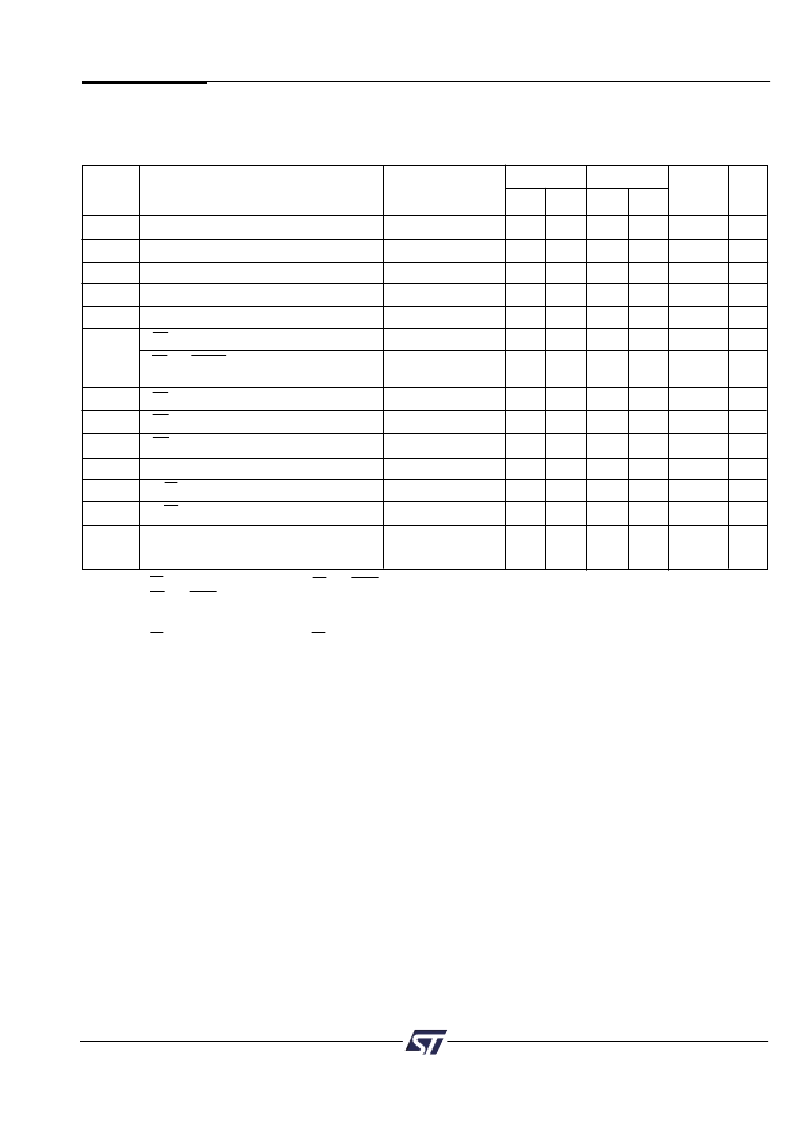
NOTES:
1.
RD timing has the same timing as DS and PSEN signals.
RD and PSEN have the same timing.
Any input used to select an internal PSD835G2 function.
In multiplexed mode, latched addresses generated from ADIO delay to address output on any Port.
RD timing has the same timing as DS.
2.
3.
4.
5.
-70
-90
Turbo
Off
Symbol
Parameter
Conditions
Min
Max
Min
Max
Unit
t
LVLX
t
AVLX
t
LXAX
t
AVQV
t
SLQV
ALE or AS Pulse Width
15
20
ns
Address Setup Time
(Note 3)
4
6
ns
Address Hold Time
(Note 3)
7
8
ns
Address Valid to Data Valid
(Note 3)
70
90
Add 12
ns
CS Valid to Data Valid
75
100
ns
RD to Data Valid
(Note 5)
24
32
ns
t
RLQV
RD or PSEN to Data Valid,
80C51 Mode
(Note 2)
31
38
ns
t
RHQX
t
RLRH
t
RHQZ
t
EHEL
t
THEH
t
ELTL
RD Data Hold Time
(Note 1)
0
0
ns
RD Pulse Width
(Note 1)
27
32
ns
RD to Data High-Z
(Note 1)
20
25
ns
E Pulse Width
27
32
ns
R/W Setup Time to Enable
6
10
ns
R/W Hold Time After Enable
0
0
ns
t
AVPV
Address Input Valid to Address
Output Delay
(Note 4)
20
25
ns
Read Timing
(5 V ± 10% Versions)
Microcontroller Interface – PSD835G2 AC/DC Parameters
(5V ±10% Versions)
發(fā)布緊急采購,3分鐘左右您將得到回復(fù)。