- 您現(xiàn)在的位置:買賣IC網(wǎng) > PDF目錄368232 > PSD835F2-15MI (意法半導(dǎo)體) Configurable Memory System on a Chip for 8-Bit Microcontrollers PDF資料下載
參數(shù)資料
| 型號: | PSD835F2-15MI |
| 廠商: | 意法半導(dǎo)體 |
| 英文描述: | Configurable Memory System on a Chip for 8-Bit Microcontrollers |
| 中文描述: | 在8片位微控制器可配置存儲(chǔ)系統(tǒng) |
| 文件頁數(shù): | 20/110頁 |
| 文件大小: | 570K |
| 代理商: | PSD835F2-15MI |
第1頁第2頁第3頁第4頁第5頁第6頁第7頁第8頁第9頁第10頁第11頁第12頁第13頁第14頁第15頁第16頁第17頁第18頁第19頁當(dāng)前第20頁第21頁第22頁第23頁第24頁第25頁第26頁第27頁第28頁第29頁第30頁第31頁第32頁第33頁第34頁第35頁第36頁第37頁第38頁第39頁第40頁第41頁第42頁第43頁第44頁第45頁第46頁第47頁第48頁第49頁第50頁第51頁第52頁第53頁第54頁第55頁第56頁第57頁第58頁第59頁第60頁第61頁第62頁第63頁第64頁第65頁第66頁第67頁第68頁第69頁第70頁第71頁第72頁第73頁第74頁第75頁第76頁第77頁第78頁第79頁第80頁第81頁第82頁第83頁第84頁第85頁第86頁第87頁第88頁第89頁第90頁第91頁第92頁第93頁第94頁第95頁第96頁第97頁第98頁第99頁第100頁第101頁第102頁第103頁第104頁第105頁第106頁第107頁第108頁第109頁第110頁
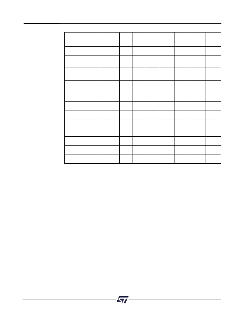
PSD835G2
PSD8XX Family
19
The
PSD835G2
Functional
Blocks
(cont.)
FS0-7
or
CSBOOT0-3
Instruction
Cycle 1 Cycle 2 Cycle 3
Cycle 4
Cycle5
Cycle 6
Cycle 7
Read (Note 5)
1
“
Read
”
RA RD
Read Main Flash ID
(Notes 6,13)
1
AAh
@555h
55h
90h
@555h
“
Read
”
ID
@x01h
@AAAh
Read Sector Protection
(Notes 6,8,13)
1
AAh
@555h
55h
90h
@555h
“
Read
”
00h or 01h
@x02h
@AAAh
Program a Flash Byte
1
AAh
@555h
55h
A0h
@555h
PD@PA
@AAAh
Erase One Flash Sector
1
AAh
@555h
55h
80h
@555h
AAh
@555h
55h
30h
@SA
30h
@AAAh
@AAAh
@next SA
(Note 7)
Erase Flash Block
(Bulk Erase)
1
AAh
@555h
55h
80h
@555h
AAh
@555h
55h
10h
@555h
@AAAh
@AAAh
Suspend Sector Erase
(Note 11)
1
B0h
@xxxh
Resume Sector Erase
(Note 12)
1
30h
@xxxh
Reset (Note 6)
1
F0 @ any
address
Unlock Bypass
1
AAh
@555h
55h
20h
@555h
@AAAh
Unlock Bypass Program
(Note 9)
1
A0h
@xxxh
PD@PA
Unlock Bypass Reset
(Note 10)
1
90h
@xxxh
00h
@xxxh
Table 8. Instructions
X
RA = Address of the memory location to be read.
RD = Data read from location RA during read operation.
PA = Address of the memory location to be programmed. Addresses are latched on the falling edge of the WR#
(CNTL0) pulse.
PD = Data to be programmed at location PA. Data is latched o the rising edge of WR# (CNTL0) pulse.
SA = Address of the sector to be erased or verified. The chip select (FS0-7 or CSBOOT0-3) of the sector to be
erased must be active (high).
= Don
’
t Care.
NOTES:
1.
All bus cycles are write bus cycle except the ones with the
“
read
”
label.
2.
All values are in hexadecimal.
3.
FS0-7 and CSBOOT0-3 are active high and are defined in PSDsoft.
4.
Only Address bits A11-A0 are used in Instruction decoding. A15-12 (or A16-A12) are don
’
t care.
5.
No unlock or command cycles required when device is in read mode.
6.
The Reset command is required to return to the read mode after reading the Flash ID, Sector Protect status
or if DQ5 (error flag) goes high.
7.
Additional sectors to be erased must be entered within 80μs.
8.
The data is 00h for an unprotected sector and 01h for a protected sector. In the fourth cycle, the sector chip
select is active and (A1 = 1, A0 = 0).
9.
The Unlock Bypass command is required prior to the Unlock Bypass Program command.
10. The Unlock Bypass Reset command is required to return to reading array data when the device is in the
Unlock Bypass mode.
11. The system may read and program functions in non-erasing sectors, read the Flash ID or read the Sector
Protect status, when in the Erase Suspend mode. The erase Suspend command is valid only during a sector
erase operation.
12. The Erase Resume command is valid only during the Erase Suspend mode.
13. The MCU cannot invoke these instructions while executing code from the same Flash memory for which the
instruction is intended. The MCU must fetch, for example, codes from the secondary block when reading the
Sector Protection Status of the main Flash.
相關(guān)PDF資料 |
PDF描述 |
|---|---|
| PSD835F2-15U | Configurable Memory System on a Chip for 8-Bit Microcontrollers |
| PSD835F2-15UI | Configurable Memory System on a Chip for 8-Bit Microcontrollers |
| PSD835F2-20B81 | Configurable Memory System on a Chip for 8-Bit Microcontrollers |
| PSD835F2-20B81I | Configurable Memory System on a Chip for 8-Bit Microcontrollers |
| PSD835F2-20J | Configurable Memory System on a Chip for 8-Bit Microcontrollers |
相關(guān)代理商/技術(shù)參數(shù) |
參數(shù)描述 |
|---|---|
| PSD835G2-70U | 功能描述:靜態(tài)隨機(jī)存取存儲(chǔ)器 5.0V 4M 70ns RoHS:否 制造商:Cypress Semiconductor 存儲(chǔ)容量:16 Mbit 組織:1 M x 16 訪問時(shí)間:55 ns 電源電壓-最大:3.6 V 電源電壓-最小:2.2 V 最大工作電流:22 uA 最大工作溫度:+ 85 C 最小工作溫度:- 40 C 安裝風(fēng)格:SMD/SMT 封裝 / 箱體:TSOP-48 封裝:Tray |
| PSD835G2-90U | 功能描述:靜態(tài)隨機(jī)存取存儲(chǔ)器 5.0V 4M 90ns RoHS:否 制造商:Cypress Semiconductor 存儲(chǔ)容量:16 Mbit 組織:1 M x 16 訪問時(shí)間:55 ns 電源電壓-最大:3.6 V 電源電壓-最小:2.2 V 最大工作電流:22 uA 最大工作溫度:+ 85 C 最小工作溫度:- 40 C 安裝風(fēng)格:SMD/SMT 封裝 / 箱體:TSOP-48 封裝:Tray |
| PSD835G2-90UI | 功能描述:靜態(tài)隨機(jī)存取存儲(chǔ)器 5.0V 4M 90ns RoHS:否 制造商:Cypress Semiconductor 存儲(chǔ)容量:16 Mbit 組織:1 M x 16 訪問時(shí)間:55 ns 電源電壓-最大:3.6 V 電源電壓-最小:2.2 V 最大工作電流:22 uA 最大工作溫度:+ 85 C 最小工作溫度:- 40 C 安裝風(fēng)格:SMD/SMT 封裝 / 箱體:TSOP-48 封裝:Tray |
| PSD835G2V-12UI | 功能描述:靜態(tài)隨機(jī)存取存儲(chǔ)器 3.0V 4M 120ns RoHS:否 制造商:Cypress Semiconductor 存儲(chǔ)容量:16 Mbit 組織:1 M x 16 訪問時(shí)間:55 ns 電源電壓-最大:3.6 V 電源電壓-最小:2.2 V 最大工作電流:22 uA 最大工作溫度:+ 85 C 最小工作溫度:- 40 C 安裝風(fēng)格:SMD/SMT 封裝 / 箱體:TSOP-48 封裝:Tray |
| PSD835G2V-90U | 功能描述:靜態(tài)隨機(jī)存取存儲(chǔ)器 3.0V 4M 90ns RoHS:否 制造商:Cypress Semiconductor 存儲(chǔ)容量:16 Mbit 組織:1 M x 16 訪問時(shí)間:55 ns 電源電壓-最大:3.6 V 電源電壓-最小:2.2 V 最大工作電流:22 uA 最大工作溫度:+ 85 C 最小工作溫度:- 40 C 安裝風(fēng)格:SMD/SMT 封裝 / 箱體:TSOP-48 封裝:Tray |
發(fā)布緊急采購,3分鐘左右您將得到回復(fù)。