- 您現(xiàn)在的位置:買賣IC網(wǎng) > PDF目錄368251 > PSD835F1V-70UI (意法半導(dǎo)體) Configurable Memory System on a Chip for 8-Bit Microcontrollers PDF資料下載
參數(shù)資料
| 型號: | PSD835F1V-70UI |
| 廠商: | 意法半導(dǎo)體 |
| 英文描述: | Configurable Memory System on a Chip for 8-Bit Microcontrollers |
| 中文描述: | 在8片位微控制器可配置存儲系統(tǒng) |
| 文件頁數(shù): | 13/110頁 |
| 文件大小: | 570K |
| 代理商: | PSD835F1V-70UI |
第1頁第2頁第3頁第4頁第5頁第6頁第7頁第8頁第9頁第10頁第11頁第12頁當前第13頁第14頁第15頁第16頁第17頁第18頁第19頁第20頁第21頁第22頁第23頁第24頁第25頁第26頁第27頁第28頁第29頁第30頁第31頁第32頁第33頁第34頁第35頁第36頁第37頁第38頁第39頁第40頁第41頁第42頁第43頁第44頁第45頁第46頁第47頁第48頁第49頁第50頁第51頁第52頁第53頁第54頁第55頁第56頁第57頁第58頁第59頁第60頁第61頁第62頁第63頁第64頁第65頁第66頁第67頁第68頁第69頁第70頁第71頁第72頁第73頁第74頁第75頁第76頁第77頁第78頁第79頁第80頁第81頁第82頁第83頁第84頁第85頁第86頁第87頁第88頁第89頁第90頁第91頁第92頁第93頁第94頁第95頁第96頁第97頁第98頁第99頁第100頁第101頁第102頁第103頁第104頁第105頁第106頁第107頁第108頁第109頁第110頁
PSD8XX Family
PSD835G2
12
Bit 7
Bit 6
Bit 5
Bit 4
Bit 3
Bit 2
Bit 1
Bit 0
Port Pin 7
Port Pin 6
Port Pin 5
Port Pin 4
Port Pin 3
Port Pin 2
Port Pin 1
Port Pin 0
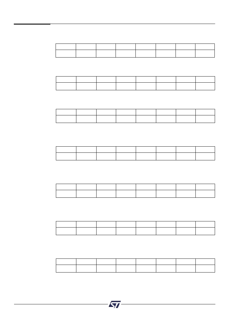
Data In Registers – Port A, B, C, D, E, F and G
8.0
Register Bit
Definition
All the registers in the PSD835G2 are included here for reference. Detail description of the
registers are found in the Functional Block section of the Data Sheet.
Bit definitions:
Read only registers, read Port pin status when Port is in MCU I/O input Mode.
Bit 7
Bit 6
Bit 5
Bit 4
Bit 3
Bit 2
Bit 1
Bit 0
Port Pin 7
Port Pin 6
Port Pin 5
Port Pin 4
Port Pin 3
Port Pin 2
Port Pin 1
Port Pin 0
Data Out Registers – Port A, B, C, D, E, F and G
Bit definitions:
Latched data for output to Port pin when pin is configured in MCU I/O output mode.
Bit 7
Bit 6
Bit 5
Bit 4
Bit 3
Bit 2
Bit 1
Bit 0
Port Pin 7
Port Pin 6
Port Pin 5
Port Pin 4
Port Pin 3
Port Pin 2
Port Pin 1
Port Pin 0
Direction Registers – Port A, B, C, D, E, F and G
Bit definitions:
Set Register Bit to 0 = configure corresponding Port pin in Input mode (default).
Set Register Bit to 1 = configure corresponding Port pin in Output mode.
Bit 7
Bit 6
Bit 5
Bit 4
Bit 3
Bit 2
Bit 1
Bit 0
Port Pin 7
Port Pin 6
Port Pin 5
Port Pin 4
Port Pin 3
Port Pin 2
Port Pin 1
Port Pin 0
Control Registers – Ports E, F and G
Bit definitions:
Set Register Bit to 0 = configure corresponding Port pin in MCU I/O mode (default).
Set Register Bit to 1 = configure corresponding Port pin in Latched Address Out mode.
Bit 7
Bit 6
Bit 5
Bit 4
Bit 3
Bit 2
Bit 1
Bit 0
Port Pin 7
Port Pin 6
Port Pin 5
Port Pin 4
Port Pin 3
Port Pin 2
Port Pin 1
Port Pin 0
Drive Registers – Ports A, B, D, E, and G
Bit definitions:
Set Register Bit to 0 = configure corresponding Port pin in CMOS output driver (default).
Set Register Bit to 1 = configure corresponding Port pin in Open Drain output driver.
Bit 7
Bit 6
Bit 5
Bit 4
Bit 3
Bit 2
Bit 1
Bit 0
Port Pin 7
Port Pin 6
Port Pin 5
Port Pin 4
Port Pin 3
Port Pin 2
Port Pin 1
Port Pin 0
Drive Registers – Ports C and F
Bit definitions:
Set Register Bit to 0 = configure corresponding Port pin as CMOS output driver (default).
Set Register Bit to 1 = configure corresponding Port pin in Slew Rate mode.
Bit 7
Bit 6
Bit 5
Bit 4
Bit 3
Bit 2
Bit 1
Bit 0
Port Pin 7
Port Pin 6
Port Pin 5
Port Pin 4
Port Pin 3
Port Pin 2
Port Pin 1
Port Pin 0
Enable Out Registers – Ports A, B, C and F
Bit definitions: Read Only Registers
Register Bit <j> = 0 indicates Port pin driver is in tri-state mode (default).
Register Bit <j> = 1 indicates Port pin driver is enabled.
相關(guān)PDF資料 |
PDF描述 |
|---|---|
| PSD835F1V-90B81 | Configurable Memory System on a Chip for 8-Bit Microcontrollers |
| PSD835F1V-90B81I | Configurable Memory System on a Chip for 8-Bit Microcontrollers |
| PSD835F1V-90J | Configurable Memory System on a Chip for 8-Bit Microcontrollers |
| PSD835F1V-90JI | Configurable Memory System on a Chip for 8-Bit Microcontrollers |
| PSD835F1V-90M | Configurable Memory System on a Chip for 8-Bit Microcontrollers |
相關(guān)代理商/技術(shù)參數(shù) |
參數(shù)描述 |
|---|---|
| PSD835G2-70U | 功能描述:靜態(tài)隨機存取存儲器 5.0V 4M 70ns RoHS:否 制造商:Cypress Semiconductor 存儲容量:16 Mbit 組織:1 M x 16 訪問時間:55 ns 電源電壓-最大:3.6 V 電源電壓-最小:2.2 V 最大工作電流:22 uA 最大工作溫度:+ 85 C 最小工作溫度:- 40 C 安裝風格:SMD/SMT 封裝 / 箱體:TSOP-48 封裝:Tray |
| PSD835G2-90U | 功能描述:靜態(tài)隨機存取存儲器 5.0V 4M 90ns RoHS:否 制造商:Cypress Semiconductor 存儲容量:16 Mbit 組織:1 M x 16 訪問時間:55 ns 電源電壓-最大:3.6 V 電源電壓-最小:2.2 V 最大工作電流:22 uA 最大工作溫度:+ 85 C 最小工作溫度:- 40 C 安裝風格:SMD/SMT 封裝 / 箱體:TSOP-48 封裝:Tray |
| PSD835G2-90UI | 功能描述:靜態(tài)隨機存取存儲器 5.0V 4M 90ns RoHS:否 制造商:Cypress Semiconductor 存儲容量:16 Mbit 組織:1 M x 16 訪問時間:55 ns 電源電壓-最大:3.6 V 電源電壓-最小:2.2 V 最大工作電流:22 uA 最大工作溫度:+ 85 C 最小工作溫度:- 40 C 安裝風格:SMD/SMT 封裝 / 箱體:TSOP-48 封裝:Tray |
| PSD835G2V-12UI | 功能描述:靜態(tài)隨機存取存儲器 3.0V 4M 120ns RoHS:否 制造商:Cypress Semiconductor 存儲容量:16 Mbit 組織:1 M x 16 訪問時間:55 ns 電源電壓-最大:3.6 V 電源電壓-最小:2.2 V 最大工作電流:22 uA 最大工作溫度:+ 85 C 最小工作溫度:- 40 C 安裝風格:SMD/SMT 封裝 / 箱體:TSOP-48 封裝:Tray |
| PSD835G2V-90U | 功能描述:靜態(tài)隨機存取存儲器 3.0V 4M 90ns RoHS:否 制造商:Cypress Semiconductor 存儲容量:16 Mbit 組織:1 M x 16 訪問時間:55 ns 電源電壓-最大:3.6 V 電源電壓-最小:2.2 V 最大工作電流:22 uA 最大工作溫度:+ 85 C 最小工作溫度:- 40 C 安裝風格:SMD/SMT 封裝 / 箱體:TSOP-48 封裝:Tray |
發(fā)布緊急采購,3分鐘左右您將得到回復(fù)。