- 您現(xiàn)在的位置:買賣IC網(wǎng) > PDF目錄368212 > PSD4235G2-B-15B81 (意法半導(dǎo)體) CAP 33UF 3V 20% TANT SMD-3216-18 TR-13-PL SN100% PDF資料下載
參數(shù)資料
| 型號: | PSD4235G2-B-15B81 |
| 廠商: | 意法半導(dǎo)體 |
| 英文描述: | CAP 33UF 3V 20% TANT SMD-3216-18 TR-13-PL SN100% |
| 中文描述: | Flash在系統(tǒng)可編程外設(shè)的16位微控制器 |
| 文件頁數(shù): | 12/93頁 |
| 文件大小: | 503K |
| 代理商: | PSD4235G2-B-15B81 |
第1頁第2頁第3頁第4頁第5頁第6頁第7頁第8頁第9頁第10頁第11頁當(dāng)前第12頁第13頁第14頁第15頁第16頁第17頁第18頁第19頁第20頁第21頁第22頁第23頁第24頁第25頁第26頁第27頁第28頁第29頁第30頁第31頁第32頁第33頁第34頁第35頁第36頁第37頁第38頁第39頁第40頁第41頁第42頁第43頁第44頁第45頁第46頁第47頁第48頁第49頁第50頁第51頁第52頁第53頁第54頁第55頁第56頁第57頁第58頁第59頁第60頁第61頁第62頁第63頁第64頁第65頁第66頁第67頁第68頁第69頁第70頁第71頁第72頁第73頁第74頁第75頁第76頁第77頁第78頁第79頁第80頁第81頁第82頁第83頁第84頁第85頁第86頁第87頁第88頁第89頁第90頁第91頁第92頁第93頁
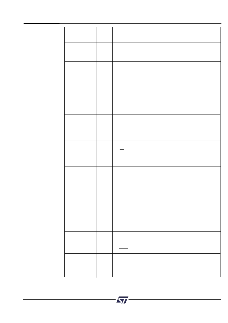
Preliminary Information
PSD4000 Series
Pin*
(TQFP
Pin Name Pkg.)
Type
Description
Reset
39
I
Active low input. Resets I/O Ports, PLD Micro
Cells, some of
the configuration registers and JTAG registers. Must be active
at power up. Reset also aborts the Flash programming/erase
cycle that is in progress.
PA0-PA7
51-58
I/O
Port A, PA0-7. This port is pin configurable and has multiple
functions:
1. MCU I/O — standard output or input port
2. GPLD output.
3. Input to the PLD (can also be PLD input for address A16
and above).
CMOS
or Open
Drain
PB0-PB7
61-68
I/O
Port B, PB0-7. This port is pin configurable and has multiple
functions:
1. MCU I/O — standard output or input port.
2. GPLD output.
3. Input to the PLD (can also be PLD input for address A16
and above).
CMOS
or Open
Drain
PC0-PC7 41-48
I/O
Port C, PC0-7. This port is pin configurable and has multiple
functions:
1. MCU I/O — standard output or input port.
2. External chip select (ECS0-7) output.
3. Input to the PLD (can also be PLD input for address A16
and above).
CMOS
or Slew
Rate
PD0
79
I/O
Port D pin PD0 can be configured as:
1. ALE or AS input — latches addresses on ADIO0-15 pins
2. AS input — latches addresses on ADIO0-15 pins on the
rising edge.
3. Input to the PLD (can also be PLD input for address A16
and above).
CMOS
or Open
Drain
PD1
80
I/O
Port D pin PD1 can be configured as:
1. MCU I/O
2. Input to the PLD (can also be PLD input for address A16
and above).
3. CLKIN clock input — clock input to the GPLD
Micro
Cells, the APD power down counter and GPLD
AND Array.
CMOS
or Open
Drain
PD2
1
I/O
Port D pin PD2 can be configured as:
1. MCU I/O
2. Input to the PLD (can also be PLD input for address A16
and above).
3. CSI input — chip select input. When low, the CSI enables
the internal PSD memories and I/O. When high, the
internal memories are disabled to conserve power. CSI
trailing edge can get the part out of power-down mode.
CMOS
or Open
Drain
PD3
2
I/O
Port D pin PD3 can be configured as:
1. MCU I/O
2. Input to the PLD (can also be PLD input for address A16
and above).
3. WRH — for 16-bit data bus, write to high byte, active low.
CMOS
or Open
Drain
PE0
71
I/O
Port E, PE0. This port is pin configurable and has multiple
functions:
1. MCU I/O — standard output or input port.
2. Latched address output.
3. TMS input for JTAG/ISP interface.
CMOS
or Open
Drain
Table 5.
PSD4000
Pin
Descriptions
(cont.)
9
相關(guān)PDF資料 |
PDF描述 |
|---|---|
| PSD4235G2-B-20JI | Flash In-System-Programmable Peripherals for 16-Bit MCUs |
| PSD4235G2-B-20M | CAP 0.47UF 25V 10% TANT SMD-3216-18 TR-13-PL GOLD |
| PSD4235G2-B-20MI | CAP 0.47UF 25V 10% TANT SMD-3216-18 TR-13-PL SN/PB5% |
| PSD4235G2-B-20U | CAP 0.47UF 25V 10% TANT SMD-3216-18 TR-13-PL SN100% |
| PSD4235G2-B-20UI | CAP 0.47UF 25V 10% TANT SMD-3216-18 TR-13-PL SN100% |
相關(guān)代理商/技術(shù)參數(shù) |
參數(shù)描述 |
|---|---|
| PSD4235G2V-12UI | 功能描述:CPLD - 復(fù)雜可編程邏輯器件 3.3V 4M 120ns RoHS:否 制造商:Lattice 系列: 存儲類型:EEPROM 大電池數(shù)量:128 最大工作頻率:333 MHz 延遲時間:2.7 ns 可編程輸入/輸出端數(shù)量:64 工作電源電壓:3.3 V 最大工作溫度:+ 90 C 最小工作溫度:0 C 封裝 / 箱體:TQFP-100 |
| PSD4235G2V-90U | 功能描述:CPLD - 復(fù)雜可編程邏輯器件 3.3V 4M 90ns RoHS:否 制造商:Lattice 系列: 存儲類型:EEPROM 大電池數(shù)量:128 最大工作頻率:333 MHz 延遲時間:2.7 ns 可編程輸入/輸出端數(shù)量:64 工作電源電壓:3.3 V 最大工作溫度:+ 90 C 最小工作溫度:0 C 封裝 / 箱體:TQFP-100 |
| PSD4256G6V-10UI | 功能描述:CPLD - 復(fù)雜可編程邏輯器件 3.3V 8M 100ns RoHS:否 制造商:Lattice 系列: 存儲類型:EEPROM 大電池數(shù)量:128 最大工作頻率:333 MHz 延遲時間:2.7 ns 可編程輸入/輸出端數(shù)量:64 工作電源電壓:3.3 V 最大工作溫度:+ 90 C 最小工作溫度:0 C 封裝 / 箱體:TQFP-100 |
| PSD4-36 | 制造商:Tamura Corporation of America 功能描述: |
| PSD-45 | 制造商:MEANWELL 制造商全稱:Mean Well Enterprises Co., Ltd. 功能描述:45W DC-DC Single Output Switching Power Supply |
發(fā)布緊急采購,3分鐘左右您將得到回復(fù)。