- 您現(xiàn)在的位置:買賣IC網(wǎng) > PDF目錄370020 > PS399CSE 4-Channel Analog Multiplexer PDF資料下載
參數(shù)資料
| 型號(hào): | PS399CSE |
| 英文描述: | 4-Channel Analog Multiplexer |
| 中文描述: | 4通道模擬多路復(fù)用器 |
| 文件頁數(shù): | 1/10頁 |
| 文件大小: | 342K |
| 代理商: | PS399CSE |

PS398/PS399
17V Analog Multiplexers
12345678901234567890123456789012123456789012345678901234567890121234567890123456789012345678901212345678901234567890123456789012123456789012
12345678901234567890123456789012123456789012345678901234567890121234567890123456789012345678901212345678901234567890123456789012123456789012
1
PS8185C 10/06/99
Features
Low On-Resistance (60Ohm typ.) Minimizes Distortion
and Error Voltages
Low Glitching Reduces Step Errors and Improves
Settling Times. Charge Injection: <5pC
Split-Supply Operation (+3V to +8V)
Improved Second Sources for MAX398/MAX399
On-Resistance Matching Between Channels: <6Ohm
On-Resistance Flatness: <11Ohm
Low Off-Channel Leakage,
I
NO(OFF)
< 1nA @ +85
o
C, I
COM(ON)
, <2.5nA @ +85
o
C
TTL/CMOS Logic Compatible
Fast Switching Speed, t
TRANS
<250ns
Break-Before-Make action eliminates momentary crosstalk
Rail-to-Rail Analog Signal Range
Low Power Consumption, <300μW
Narrow SOIC and QSOP Packages Minimize Board Area
Applications
Data Acquisition Systems
Audio Switching and Routing
Test Equipment
PBX, PABX
Telecommunication Systems
Battery-Powered Systems
Description
The PS398/PS399 are improved high precision analog multiplexers.
The PS398, an 8-channel single-ended mux, selects one of eight
inputs to a common output as determined by a 3-bit address
A0-A2. An EN (enable) pin when low disables all switches, use-
ful when stacking several devices. The PS399 is a 4-channel
differential multiplexer. It selects one of four differential inputs to
a common differential output as determined by a 2-bit address A0,
A1. An EN pin may be driven low to disable all switches.
These multiplexers operate with dual supplies from +3V to +8V.
Single-supply operation is possible from +3V to +15V.
With +5V power supplies, the PS398/PS399 guarantee <100Ohm
on-resistance
.
On-resistance matching between channels is within
6Ohm. On-resistance flatness is less than 11Ohm
over the speci-
fied signal range.
Each switch conducts current equally well in either direction when
on. In the off state each switch blocks voltages up to the power-
supply rails.
Both devices guarantee low leakage currents (<2.5nA at +85
o
C)
and fast switching speeds (t
TRANS
<250ns). Break-before-make
switching action protects against momentary crosstalk between
channels.
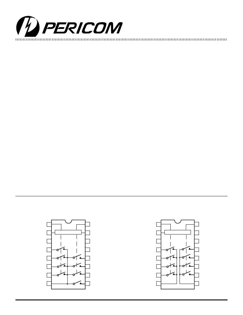
Functional Block Diagrams and Pin Configurations
8
Decoders/Drivers
1
2
3
4
5
6
7
9
16
15
14
13
12
11
10
A0
EN
V-
NO1
NO2
NO3
NO4
COM
A1
A2
GND
V+
NO5
NO6
NO7
NO8
8
Decoders/Drivers
1
2
3
4
5
6
7
9
16
15
14
13
12
11
10
AO
EN
V-
NO1A
NO2A
NO3A
NO4A
COMA
A1
GND
V+
NO1B
NO2B
NO3B
NO4B
COMB
Top View
PS398
Top View
PS399
相關(guān)PDF資料 |
PDF描述 |
|---|---|
| PS399EEE | 4-Channel Analog Multiplexer |
| PS399EPE | 4-Channel Analog Multiplexer |
| PS399ESE | 4-Channel Analog Multiplexer |
| PS398 | Analog | 8-Channel Mux |
| PS399 | Analog | 4-Channel Differential Mux |
相關(guān)代理商/技術(shù)參數(shù) |
參數(shù)描述 |
|---|---|
| PS399CSEE | 功能描述:多路器開關(guān) IC Precision Diff 4Ch 17V Analog RoHS:否 制造商:Texas Instruments 通道數(shù)量:1 開關(guān)數(shù)量:4 開啟電阻(最大值):7 Ohms 開啟時(shí)間(最大值): 關(guān)閉時(shí)間(最大值): 傳播延遲時(shí)間:0.25 ns 工作電源電壓:2.3 V to 3.6 V 工作電源電流: 最大工作溫度:+ 85 C 安裝風(fēng)格:SMD/SMT 封裝 / 箱體:UQFN-16 |
| PS399CSEEX | 功能描述:多路器開關(guān) IC Precision Diff 4Ch 17V Analog RoHS:否 制造商:Texas Instruments 通道數(shù)量:1 開關(guān)數(shù)量:4 開啟電阻(最大值):7 Ohms 開啟時(shí)間(最大值): 關(guān)閉時(shí)間(最大值): 傳播延遲時(shí)間:0.25 ns 工作電源電壓:2.3 V to 3.6 V 工作電源電流: 最大工作溫度:+ 85 C 安裝風(fēng)格:SMD/SMT 封裝 / 箱體:UQFN-16 |
| PS399CSEX | 制造商:Pericom Semiconductor Corporation 功能描述:Analog Multiplexer Single 4:1 16-Pin SOIC T/R |
| PS399EEE | 制造商:未知廠家 制造商全稱:未知廠家 功能描述:4-Channel Analog Multiplexer |
| PS399EPE | 制造商:未知廠家 制造商全稱:未知廠家 功能描述:4-Channel Analog Multiplexer |
發(fā)布緊急采購,3分鐘左右您將得到回復(fù)。