- 您現(xiàn)在的位置:買賣IC網(wǎng) > PDF目錄368105 > PQXXRA11SERIES LOW POWER-LOSS VOLTAGE REGULATORS PDF資料下載
參數(shù)資料
| 型號(hào): | PQXXRA11SERIES |
| 英文描述: | LOW POWER-LOSS VOLTAGE REGULATORS |
| 中文描述: | 低功率損耗的電壓調(diào)節(jié)器 |
| 文件頁(yè)數(shù): | 2/7頁(yè) |
| 文件大小: | 67K |
| 代理商: | PQXXRA11SERIES |
Low Power-Loss Voltage Regulators
PQ05RD21 Series/PQ3RD23
I
Electrical Characteristics
Parameter
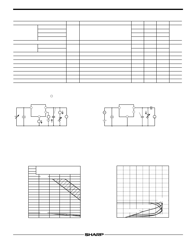
Fig. 1 Test Circuit
Fig. 2 Test Circuit of Ripple Rejection
Symbol
Conditions
MIN.
3.201
TYP.
3.3
MAX.
3.399
Unit
Output voltage
4.85
8.73
11.64
5.0
9.0
12.0
5.15
9.27
12.36
V
Load regulation
Io=5mA to 2.0A,
4
––
––
––
0.1
0.1
0.5
2.0
2.5
2.5
%
Line regulation
5
, I
O
=5mA
––
%
Temperature coefficient of output voltage
Ripple rejection
Dropout voltage
7
ON-state voltage for control
ON-state current for control
Tj=0 to 125
C, Io=5mA
Refer to Fig.2
6
, Io=2A
––
45
––
2.0
––
––
––
±
0.02
55
––
––
––
––
––
––
––
0.5
––
%/
C
dB
V
V
μ
A
4
4
V
C
=2.7V,
4
4
V
C
=0.4V,
4
OFF-state voltage for control
OFF-state current for control
0.8
–
0.4
V
Quiescent current
I
O
=0A,
4
––
10
mA
mA
20
4
PQ3RD23
:V
IN
=5V,
PQ05RD21
:V
IN
=7V,
PQ09RD21
:V
IN
=11V,
PQ12RD21
: V
IN
=14V
5
PQ3RD23
:V
IN
=4 to 10V,
PQ05RD21
:V
IN
= 6 to 12V,
PQ09RD21
:V
IN
=10 to 16V,
PQ12RD21
: V
IN
=13 to 19V
6
Input voltage shall be the value when output voltage is 95% in comparison with the initial value.
PQ3RD23
:V
IN
=3.7V
7
In case of opening control teminal , output voltage turns on.
4
PQ05RD21
PQ09RD21
PQ12RD21
(Unless otherwise specified, Io=1.0A,
4
, T
a
=25
C)
PQ3RD23
PQ3RD23
PQ05RD21 series
V
O
R
eg
L
R
eg
I
T
C
V
O
RR
V
i
-
O
V
C
(
ON
)
I
C
(
ON
)
V
C
(
OFF
)
I
C
(
OFF
)
I
q
A
V
A
A
V
IN
I
q
I
C
I
O
V
O
V
C
R
L
0.33
μ
F
47
μ
F
+
1
2
3
4
e
i
V
IN
I
O
e
o
R
L
0.33
μ
F
47
μ
F
+
+
f=120Hz (sine wave)
e
i(rms)
=0.5V
V
IN
=5V (
PQ3RD23
)
7V (
PQ05RD21
)
11V (
PQ09RD21
)
14V (
PQ12RD21
)
I
O
=0.5A
RR=20 log (e
i(rms)
/e
o(rms)
)
1
2
3
4
V
Fig. 4 Overcurrent Protection
Characteristics (Typical Value)
(PQ3RD23)
12
Fig. 3 Power Dissipation vs. Ambient
Temperature
20
0
5
10
15
–
20
0
20
40
60
80
P
D2
P
D1
P
D
(
Ambient temperature T
a
(
C)
Note)
Oblique line portion : Overheat protection may operate in this area.
P
D1
:No heat sink
P
D2
:With infinite heat sink
O
O
(
Output current I
O
(A)
0
1.0
3.0
4.0
2.0
1
2
3
4
7
6
8
9
5
10
11
V
i
-
O
=3V
V
i
-
O
=1V
V
i
-
O
=0.5V
V
i
-
O
=2V
相關(guān)PDF資料 |
PDF描述 |
|---|---|
| PQXXRA1SERIES | LOW POWER-LOSS VOLTAGE REGULATORS |
| PQXXRD08SERIES | LOW POWER-LOSS VOLTAGE REGULATORS |
| PQXXRD11SERIES | LOW POWER-LOSS VOLTAGE REGULATORS |
| PQXXRD21SERIES | LOW POWER-LOSS VOLTAGE REGULATORS |
| PQXXRF11SERIES | LOW POWER-LOSS VOLTAGE REGULATORS |
相關(guān)代理商/技術(shù)參數(shù) |
參數(shù)描述 |
|---|---|
| PQXXRA1SERIES | 制造商:未知廠家 制造商全稱:未知廠家 功能描述:LOW POWER-LOSS VOLTAGE REGULATORS |
| PQXXRD08SERIES | 制造商:未知廠家 制造商全稱:未知廠家 功能描述:LOW POWER-LOSS VOLTAGE REGULATORS |
| PQXXRD11SERIES | 制造商:未知廠家 制造商全稱:未知廠家 功能描述:LOW POWER-LOSS VOLTAGE REGULATORS |
| PQXXRD21SERIES | 制造商:未知廠家 制造商全稱:未知廠家 功能描述:LOW POWER-LOSS VOLTAGE REGULATORS |
| PQXXRF11SERIES | 制造商:未知廠家 制造商全稱:未知廠家 功能描述:LOW POWER-LOSS VOLTAGE REGULATORS |
發(fā)布緊急采購(gòu),3分鐘左右您將得到回復(fù)。