- 您現(xiàn)在的位置:買賣IC網(wǎng) > PDF目錄368097 > PPC440GX-3FF533C (APPLIEDMICRO INC) Power PC 440GX Embedded Processor PDF資料下載
參數(shù)資料
| 型號: | PPC440GX-3FF533C |
| 廠商: | APPLIEDMICRO INC |
| 元件分類: | 微控制器/微處理器 |
| 英文描述: | Power PC 440GX Embedded Processor |
| 中文描述: | 32-BIT, 533 MHz, RISC PROCESSOR, PBGA552 |
| 封裝: | 25 X 25 MM, PLASTIC, FBGA-552 |
| 文件頁數(shù): | 78/93頁 |
| 文件大小: | 794K |
| 代理商: | PPC440GX-3FF533C |
第1頁第2頁第3頁第4頁第5頁第6頁第7頁第8頁第9頁第10頁第11頁第12頁第13頁第14頁第15頁第16頁第17頁第18頁第19頁第20頁第21頁第22頁第23頁第24頁第25頁第26頁第27頁第28頁第29頁第30頁第31頁第32頁第33頁第34頁第35頁第36頁第37頁第38頁第39頁第40頁第41頁第42頁第43頁第44頁第45頁第46頁第47頁第48頁第49頁第50頁第51頁第52頁第53頁第54頁第55頁第56頁第57頁第58頁第59頁第60頁第61頁第62頁第63頁第64頁第65頁第66頁第67頁第68頁第69頁第70頁第71頁第72頁第73頁第74頁第75頁第76頁第77頁當前第78頁第79頁第80頁第81頁第82頁第83頁第84頁第85頁第86頁第87頁第88頁第89頁第90頁第91頁第92頁第93頁
440GX – Power PC 440GX Embedded Processor
78
AMCC
Revision 1.15 – August 30, 2007
Data Sheet
DDR SDRAM I/O Specifications
The DDR SDRAM controller times its operation with internal PLB clock signals and generates MemClkOut0 from
the PLB clock. The PLB clock is an internal signal that cannot be directly observed. However MemClkOut0 is the
same frequency as the PLB clock signal and is in phase with the PLB clock signal.
Note:
MemClkOut0 can be advanced with respect to the PLB clock by means of the SDRAM0_CLKTR program-
ming register. In a typical system, users advance MemClkOut by 90
°
. This depends on the specific applica-
tion and requires a thorough understanding of the memory system in general (refer to the DDR SDRAM
controller chapter in the
PowerPC 440GX User’s Manual
).
In the following sections, the label MemClkOut0(0) refers to MemClkOut0 when it has not been phase-shifted, and
MemClkOut0(90) refers to MemClkOut0 when it has been phase-advanced 90
°
. Advancing MemClkOut0 by 90
°
creates a 3/4 cycle setup time and 1/4 cycle hold time for the address and control signals in relation to
MemClkOut0(90). The rising edge of MemClkOut0(90) aligns with the first rising edge of the DQS signal.
The following DDR data is generated by means of simulation and includes logic, driver, package RLC, and lengths.
Values are calculated over best case and worst case processes with speed, temperature, and voltage as follows:
Best Case = Fast process, -40
°
C, +1.6V
Worst Case = Slow process, +85
°
C, +1.4V
Note:
In all the following DDR tables and timing diagrams,
minimum
values are measured under
best
case condi-
tions and
maximum
values are measured under
worst
case conditions.
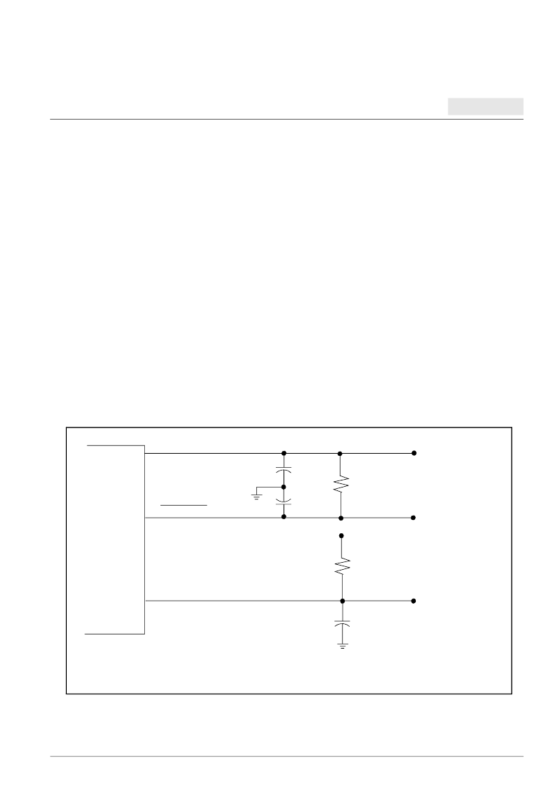
The signals are terminated as indicated in the figure below for the DDR timing data in the following sections.
DDR SDRAM Simulation Signal Termination Model
10pF
10pF
MemClkOut0
MemClkOut0
120
Ω
50
Ω
Addr/Ctrl/Data/DQS
V
TT
= SV
DD
/2
PPC440GX
30pF
Note:
This diagram illustrates the model of the DDR SDRAM interface used when generating simulation timing data.
It is
not
a recommended physical circuit design for this interface. An actual interface design will depend on many
factors, including the type of memory used and the board layout.
相關PDF資料 |
PDF描述 |
|---|---|
| PPC440GX-3FF533E | Power PC 440GX Embedded Processor |
| PPC440GX-3FF667C | Power PC 440GX Embedded Processor |
| PPC440GX-3FF667E | Power PC 440GX Embedded Processor |
| PPC440GX-3RF400C | Power PC 440GX Embedded Processor |
| PPC440GX-3RF533C | Power PC 440GX Embedded Processor |
相關代理商/技術參數(shù) |
參數(shù)描述 |
|---|---|
| PPC440GX-3FF533CZ | 制造商:AppliedMicro 功能描述:MPU 440GX RISC 32BIT 0.13UM 533MHZ 3.3V 552FCBGA - Tape and Reel |
| PPC440GX-3FF533E | 制造商:AppliedMicro 功能描述: |
| PPC440GX-3FF667C | 制造商:AMCC 制造商全稱:Applied Micro Circuits Corporation 功能描述:Power PC 440GX Embedded Processor |
| PPC440GX-3FF667CZ | 制造商:AppliedMicro 功能描述:MPU 440GX RISC 32BIT 0.13UM 667MHZ 3.3V 552FCBGA - Tape and Reel |
| PPC440GX-3FF667E | 制造商:AMCC 制造商全稱:Applied Micro Circuits Corporation 功能描述:Power PC 440GX Embedded Processor |
發(fā)布緊急采購,3分鐘左右您將得到回復。