- 您現(xiàn)在的位置:買賣IC網(wǎng) > PDF目錄378056 > PM7375-SC (PMC-SIERRA INC) LOCAL ATM SAR & PHYSICAL LAYER PDF資料下載
參數(shù)資料
| 型號: | PM7375-SC |
| 廠商: | PMC-SIERRA INC |
| 元件分類: | 數(shù)字傳輸電路 |
| 英文描述: | LOCAL ATM SAR & PHYSICAL LAYER |
| 中文描述: | ATM SEGMENTATION AND REASSEMBLY DEVICE, PQFP208 |
| 封裝: | 28 X 28 MM, 3.49 MM HEIGHT, 0.50 MM PITCH, METRIC, PLASTIC, QFP-208 |
| 文件頁數(shù): | 1/2頁 |
| 文件大小: | 119K |
| 代理商: | PM7375-SC |
PMC-931138 (R6)
1998 PMC-Sierra, Inc. October, 1998
PM7375
LASAR-155
PMC-Sierra,Inc.
ATM SAR and PHY Processor for PCI Bus
FEATURES
Combines PHY, ATM, AAL5, and PCI
DMA Controller on a single device to
simplify the design, programming, and
manufacturing of ATM adapters.
Conforms to ATM Forum User-
Network Interface (UNI) Specification
Version 3.1, Bellcore Standard TA-
NWT-001113, and ITU-T
Recommendations I.432 and I.363.
HOST INTERFACE
Provides a 32-bit, 33 MHz Peripheral
Component Interconnect (PCI) Local
Bus Specifications Version 2.1
interface and supports both bus-
master and bus-slave access modes.
Other 32-bit system buses can be
accommodated using external glue
logic.
Implements an efficient DMA controller
to manage the transfer of packets
between the SAR engine and the host
memory with minimum PCI Host
intervention. There is no need for a
local packet memory.
The transmit and receive DMA
channels support scatter/gather
capabilities where a packet can be
stored in non-contiguous buffers.
Provides an 8-cell FIFO in the transmit
direction and a 96-cell FIFO in the
receive direction to allow for up to
270
μ
s of PCI bus latency in the
receive direction.
PHYSICAL LAYER
Incorporates the industry standard
PMC PM5346 S/UNI
-LITE to provide
SONET and SDH interfaces at STS-
3c/STM-1 (155.52 Mb/s) and STS-1
(51.84 Mb/s) rates.
Provides on-chip clock recovery and
clock synthesis units that are compliant
with Bellcore TR-NWT-000253 Issue 2
and ITU-T Recommendation G.958
jitter requirements.
Performs SONET/SDH framer,
overhead, and cell processing
functions at STS-3c/STM-1 and STS-1
rates.
ATM AND ADAPTATION
LAYERS
Supports the simultaneous
segmentation and reassembly of 128
open Virtual Circuits (VCs) in both
transmit and receive directions.
Provides leaky bucket Peak Cell Rate
(PCR) enforcement using eight
programmable peak queues coupled
with sub-rate control on a per-VC
basis.
Implements Sustainable Cell Rate
(SCR) enforcement using a token
generation mechanism on a per-VC
basis.
Provides an internal VC parameter
storage for both the 128 transmit and
128 receive VCs to simplify the design
of the ATM adapter and to sustain a
high data throughput rate.
MULTIPURPOSE PORT
In bypass mode, provides an 8-bit
SCI-PHY
or UTOPIA-compliant port
to connect to an external physical layer
processor such as PM7345 S/UNI-
PDH
for DS3/E3 UNI.
In non-bypass mode, supports the
insertion and extraction of Constant Bit
Rate (CBR) cells that carry encoded
video and audio signals.
MICROPROCESSOR
INTERFACE
In slave mode, provides a generic 8-bit
microprocessor port for the
configuration, control, and monitoring
by an optional microprocessor.
In master mode, allows for the control
of two external devices without glue
logic.
PACKAGING
Provides a standard 5-signal P1149.1
JTAG test port for boundary scan
board test purposes.
Implemented in low power, 0.6 micron,
+5 V CMOS technology with TTL and
Pseudo ECL (PECL) compatible inputs
and outputs.
Packaged in 208-pin Plastic Quad Flat
Pack (PQFP) package.
APPLICATIONS
ATM Workstations and Adapters
ATM Bridges, Switches, and Hubs
Multimedia Terminals
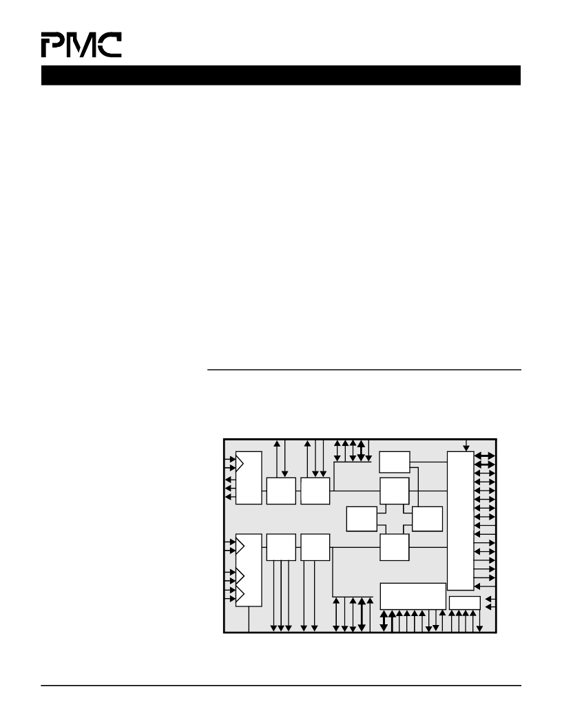
BLOCK DIAGRAM
D
A
A
C
W
R
R
Microprocessor
Interface
I
PCIINTB
PCICLK
PERRB
SERRB
REQB
GNTB
Receive
ATM Cell
Processor
Receive
Framer and
Overhead
Processor
T
T
X
T
T
R
R
R
R
R
Receive
Line
Interface
RRCLK-
ALOS+
ALOS-
RRCLK+
RXD-
RXD+
TXC
TXD-
TXD+
Receive
ATM and
Adaptation
Processor
SAR
Perfor-
mance
Monitor
Connection
Parameter
Store
Transmit
ATM Traffic
Shaper
TRCLK-
TRCLK+
JTAG Port
Transmit
Framer and
Overhead
Processor
Transmit
ATM Cell
Processor
Transmit
Line
Interface
Transmit
ATM and
Adaptation
Processor
R
R
R
R
R
R
T
T
T
T
T
M
L
R
T
T
T
T
T
DEVSELB
IDSEL
IRDBY
STOPB
FRAMEB
TRDYB
LOCKB
PCI
DMA
Controller
PAR
AD[31:0]
C/BEB[3:0]
PCICLKO
SYSCLK
相關(guān)PDF資料 |
PDF描述 |
|---|---|
| PM7380 | FRAME ENGINE AND DATA LINK MANAGER 32P672 |
| PM7380-PI | FRAME ENGINE AND DATA LINK MANAGER 32P672 |
| PM7381 | Frame Engine and Data Link Manager |
| PM7381-PI | 32 LINK, 672 CHANNEL FRAME ENGINE AND DATA LINK MANAGER WITH ANY-PHY PACKET INTERFACE |
| PM7382-PI | FRAME ENGINE AND DATA LINK MANAGER 32P256 |
相關(guān)代理商/技術(shù)參數(shù) |
參數(shù)描述 |
|---|---|
| PM7375-SGC | 制造商:PMC Sierra from Components Direct 功能描述:PM7375-SGC - Trays 制造商:PMC-Sierra 功能描述:PMC-Sierra PM7375-SGC Communication Misc |
| PM7380 | 制造商:PMC 制造商全稱:PMC 功能描述:Frame Engine and Data Link Manager |
| PM7380-PI | 制造商:PMC 制造商全稱:PMC 功能描述:FRAME ENGINE AND DATA LINK MANAGER 32P672 |
| PM7381 | 制造商:PMC 制造商全稱:PMC 功能描述:32 LINK, 672 CHANNEL FRAME ENGINE AND DATA LINK MANAGER WITH ANY-PHY PACKET INTERFACE |
發(fā)布緊急采購,3分鐘左右您將得到回復。