- 您現(xiàn)在的位置:買賣IC網(wǎng) > PDF目錄368048 > PLL500-17DC (Electronic Theatre Controls, Inc.) Low Phase Noise VCXO (17MHz to 36MHz) PDF資料下載
參數(shù)資料
| 型號(hào): | PLL500-17DC |
| 廠商: | Electronic Theatre Controls, Inc. |
| 英文描述: | Low Phase Noise VCXO (17MHz to 36MHz) |
| 中文描述: | 低相位噪聲壓控振蕩器(17MHz至36MHz基本) |
| 文件頁(yè)數(shù): | 3/6頁(yè) |
| 文件大小: | 215K |
| 代理商: | PLL500-17DC |
PLL500-17
Low Phase Noise VCXO (17MHz to 36MHz)
47745 Fremont Blvd., Fremont, California 94538 Tel (510) 492-0990 Fax (510) 492-0991
www.phaselink.com
Rev 03/29/05 Page 3
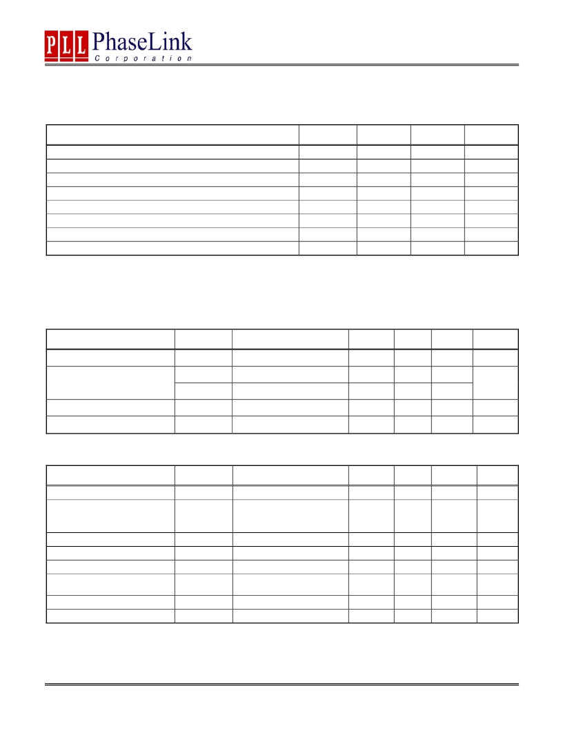
ELECTRICAL SPECIFICATIONS
1. Absolute Maximum Ratings
PARAMETERS
SYMBOL
MIN.
MAX.
UNITS
Supply Voltage
Input Voltage, dc
Output Voltage, dc
Storage Temperature
Ambient Operating Temperature*
Junction Temperature
Lead Temperature (soldering, 10s)
ESD Protection, Human Body Model
V
DD
V
I
V
O
T
S
T
A
T
J
4.6
V
V
V
°
C
°
C
°
C
°
C
kV
-0.5
-0.5
-65
-40
V
DD
+0.5
V
DD
+0.5
150
85
125
260
2
Exposure of the device under conditions beyond the limits specified by Maximum Ratings for extended periods may cause permanent damage to the
device and affect product reliability. These conditions represent a stress rating only, and functional operations of the device at these or any other
conditions above the operational limits noted in this specification is not implied.
*
Note
: Operating Temperature is guaranteed by design for all parts (COMMERCIAL and INDUSTRIAL), but tested for COMMERCIAL grade only.
2. AC Electrical Specifications
PARAMETERS
SYMBOL
CONDITIONS
MIN.
TYP.
MAX.
UNITS
Input Crystal Frequency
17
36
MHz
0.8V ~ 2.0V with 10 pF load
1.15
Output Clock Rise/Fall Time
0.3V ~ 3.0V with 15 pF load
3.7
ns
Output Clock Duty Cycle
Measured @ 1.4V
45
50
55
%
Short Circuit Current
±
50
mA
3. Voltage Control Crystal Oscillator
PARAMETERS
SYMBOL
CONDITIONS
MIN.
TYP.
MAX.
UNITS
VCXO Stabilization Time *
T
VCXOSTB
From power valid
F
XIN
= 12 – 25MHz;
XTAL C
0
/C
1
< 250
0V
≤
VCON
≤
3.3V
VCON=1.65V,
±
1.65V
Frequency change with
VDD varied +/- 10%
0V
≤
VCON
≤
3.3V, -3dB
10
ms
VCXO Tuning Range
300
ppm
CLK output pullability
VCXO Tuning Characteristic
Pull range linearity
±
150
ppm
ppm/V
%
100
5
Power Supply Rejection
PWSRR
-1
+1
ppm
VCON pin input impedance
VCON modulation BW
2000
45
k
kHz
Note:
Parameters denoted with an asterisk (*) represent nominal characterization data and are not production tested to any specific limits.
4. Jitter and Phase Noise Specifications
相關(guān)PDF資料 |
PDF描述 |
|---|---|
| PLL500-17SC | Low Phase Noise VCXO (17MHz to 36MHz) |
| PLL500-17SCL | Low Phase Noise VCXO (17MHz to 36MHz) |
| PLL500-17SCL-R | Low Phase Noise VCXO (17MHz to 36MHz) |
| PLL500-17SC-R | Low Phase Noise VCXO (17MHz to 36MHz) |
| PLL502-02 | Low Phase Noise VCXO (24MHz to 50MHz) |
相關(guān)代理商/技術(shù)參數(shù) |
參數(shù)描述 |
|---|---|
| PLL500-17DCL | 制造商:PLL 制造商全稱:PLL 功能描述:Low Phase Noise VCXO (17MHz to 36MHz) |
| PLL500-17DCLR | 制造商:PLL 制造商全稱:PLL 功能描述:Low Phase Noise VCXO (17MHz to 36MHz) |
| PLL500-17DCR | 制造商:PLL 制造商全稱:PLL 功能描述:Low Phase Noise VCXO (17MHz to 36MHz) |
| PLL500-17DI | 制造商:PLL 制造商全稱:PLL 功能描述:Low Phase Noise VCXO (17MHz to 36MHz) |
| PLL500-17DIL | 制造商:PLL 制造商全稱:PLL 功能描述:Low Phase Noise VCXO (17MHz to 36MHz) |
發(fā)布緊急采購(gòu),3分鐘左右您將得到回復(fù)。