- 您現(xiàn)在的位置:買賣IC網(wǎng) > PDF目錄368033 > PJ7920CI (Electronic Theatre Controls, Inc.) 3-Terminal Negative Output Voltage Regulators PDF資料下載
參數(shù)資料
| 型號: | PJ7920CI |
| 廠商: | Electronic Theatre Controls, Inc. |
| 英文描述: | 3-Terminal Negative Output Voltage Regulators |
| 中文描述: | 三端負(fù)輸出電壓調(diào)節(jié)器 |
| 文件頁數(shù): | 5/9頁 |
| 文件大小: | 354K |
| 代理商: | PJ7920CI |
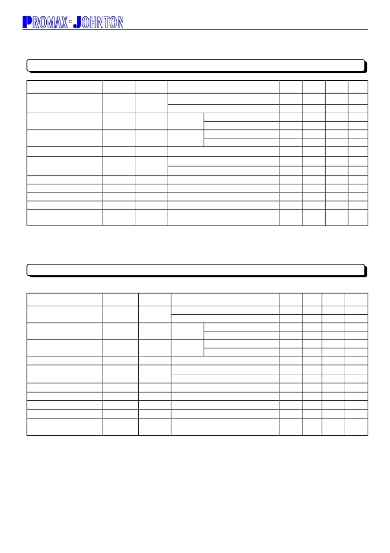
PJ7900 Series
3-Terminal Negative Output Voltage Regulators
5-9
2002/10.rev.A
(Vin=-23V, Iout=500mA, Cin=2
μ
F, Cout=1
μ
F; Tj=0
℃
to 125
℃
, unless otherwise specified.)
TEST
CIRCUIT
CHARACTERISTIC
SYMBOL
CONDITION
MIN.
TYP.
MAX.
UNI
T
V
Tj=25
℃
-14.42
-15
-15.60
Output Voltage
Vo
1
Vi=-17.5 to -30V, Io=5mA to 1A, P
D
<15W
Tj=25
℃
Vi=-17.5 to -30V
Vi=-20 to -26V
Tj=25
℃
Io=5mA to 1.5A
Io=250mA to 750mA
Tj=25
℃
-14.28
--
--
--
--
--
-15
11
3
12
4
2.5
-15.75
300
150
300
150
5
V
mV
mV
mV
mV
mA
Line Regulation
REGline
1
Load Regulation
REGload
1
Quiescent Current
Iq
2
Vi=-17.5 to -30V
--
--
1
mA
Quiescent Current Change
Δ
Iq
2
lo=5mA to 1A
f=10Hz to 100KHz, Ta=25
℃
Vi=-18.5 to -28.5V, Io=100mA, f=120Hz
Io=1A, Tj=25
℃
Tj=25
℃
--
--
54
--
--
--
90
69
1.1
2.1
0.5
--
--
--
--
mA
μ
V
dB
V
A
mV/
℃
Output Noise Voltage
Ripple Rejection Ratio
Min. I/O Voltage Difference
Peak Output Current
Output Voltage
Tempoerature Coefficient
Vn
RR
Vdif
Io-peak
1
3
1
Δ
Vo/Ta
1
Io=5mA, Tj=0 to 125
℃
--
-0.9
--
Note: The specified condition Tj=25
℃
means that the test should be carried out with the test time so short (within 10mS), that the drift in
characteristic value due to the rise in chip junction temperature can be ignored.
(Vin=-27V, Iout=500mA, Cin=2
μ
F, Cout=1
μ
F; Tj=0
℃
to 125
℃
, unless otherwise specified.)
CHARACTERISTIC
SYMBOL
TEST
CIRCUIT
CONDITION
MIN.
-17.30
-17.14
--
--
--
--
--
--
--
--
53
--
--
--
TYP.
-18
-18
15
5
12
4
2.5
--
--
110
68
1.1
2.1
-1
MAX.
-18.72
-18.90
360
180
360
180
5
1
0.5
--
--
--
--
UNIT
V
V
mV
mV
mV
mV
mA
mA
mA
μ
V
dB
V
A
mV/
℃
Tj=25
℃
Vi=-21 to -33V, Io=5mA to 1A, P
D
<15W
Tj=25
℃
Vi=-21 to -33V
Vi=-24 to -30V
Tj=25
℃
Io=5mA to 1.5A
Io=250mA to 750mA
Tj=25
℃
Vi=-21 to -33V, Tj=25
℃
lo=5mA to 1.5A, Tj=25
℃
f=10Hz to 100KHz, Ta=25
℃
Vi=-22 to -32V, Io=100mA, f=120Hz
Io=1A, Tj=25
℃
Tj=25
℃
Io=5mA, Tj=0 to 125
℃
Output Voltage
Vo
1
Line Regulation
REGline
1
Load Regulation
REGload
1
Quiescent Current
I
q
2
Quiescent Current Change
Δ
Iq
2
Output Noise Voltage
Ripple Rejection Ratio
Min. I/O Voltage Difference
Peak Output Current
Output Voltage
Tempoerature Coefficient
Vn
RR
Vdif
Io-peak
Δ
Vo/Ta
1
3
1
1
--
Note: The specified condition Tj=25
℃
means that the test should be carried out with the test time so short (within 10mS), that the drift in
characteristic value due to the rise in chip junction temperature can be ignored.
PJ7918 ELECTRICAL CHARACTERISTICS
PJ7915 ELECTRICAL CHARACTERISTICS
相關(guān)PDF資料 |
PDF描述 |
|---|---|
| PJ7920CZ | 3-Terminal Negative Output Voltage Regulators |
| PJ7921CI | 3-Terminal Negative Output Voltage Regulators |
| PJ7921CZ | 3-Terminal Negative Output Voltage Regulators |
| PJ7922CI | 3-Terminal Negative Output Voltage Regulators |
| PJ7922CZ | 3-Terminal Negative Output Voltage Regulators |
相關(guān)代理商/技術(shù)參數(shù) |
參數(shù)描述 |
|---|---|
| PJ7920CZ | 制造商:未知廠家 制造商全稱:未知廠家 功能描述:3-Terminal Negative Output Voltage Regulators |
| PJ7921CI | 制造商:未知廠家 制造商全稱:未知廠家 功能描述:3-Terminal Negative Output Voltage Regulators |
| PJ7921CZ | 制造商:未知廠家 制造商全稱:未知廠家 功能描述:3-Terminal Negative Output Voltage Regulators |
| PJ7922CI | 制造商:未知廠家 制造商全稱:未知廠家 功能描述:3-Terminal Negative Output Voltage Regulators |
| PJ7922CZ | 制造商:未知廠家 制造商全稱:未知廠家 功能描述:3-Terminal Negative Output Voltage Regulators |
發(fā)布緊急采購,3分鐘左右您將得到回復(fù)。