- 您現(xiàn)在的位置:買賣IC網(wǎng) > PDF目錄10853 > PIC16LV54AT-02/SO (Microchip Technology)IC MCU OTP 512X12 18SOIC PDF資料下載
參數(shù)資料
| 型號: | PIC16LV54AT-02/SO |
| 廠商: | Microchip Technology |
| 文件頁數(shù): | 36/194頁 |
| 文件大?。?/td> | 0K |
| 描述: | IC MCU OTP 512X12 18SOIC |
| 標準包裝: | 1,100 |
| 系列: | PIC® 16C |
| 核心處理器: | PIC |
| 芯體尺寸: | 8-位 |
| 速度: | 2MHz |
| 外圍設備: | POR,WDT |
| 輸入/輸出數(shù): | 12 |
| 程序存儲器容量: | 768B(512 x 12) |
| 程序存儲器類型: | OTP |
| RAM 容量: | 25 x 8 |
| 電壓 - 電源 (Vcc/Vdd): | 2 V ~ 3.8 V |
| 振蕩器型: | 外部 |
| 工作溫度: | 0°C ~ 70°C |
| 封裝/外殼: | 18-SOIC(0.295",7.50mm 寬) |
| 包裝: | 帶卷 (TR) |
第1頁第2頁第3頁第4頁第5頁第6頁第7頁第8頁第9頁第10頁第11頁第12頁第13頁第14頁第15頁第16頁第17頁第18頁第19頁第20頁第21頁第22頁第23頁第24頁第25頁第26頁第27頁第28頁第29頁第30頁第31頁第32頁第33頁第34頁第35頁當前第36頁第37頁第38頁第39頁第40頁第41頁第42頁第43頁第44頁第45頁第46頁第47頁第48頁第49頁第50頁第51頁第52頁第53頁第54頁第55頁第56頁第57頁第58頁第59頁第60頁第61頁第62頁第63頁第64頁第65頁第66頁第67頁第68頁第69頁第70頁第71頁第72頁第73頁第74頁第75頁第76頁第77頁第78頁第79頁第80頁第81頁第82頁第83頁第84頁第85頁第86頁第87頁第88頁第89頁第90頁第91頁第92頁第93頁第94頁第95頁第96頁第97頁第98頁第99頁第100頁第101頁第102頁第103頁第104頁第105頁第106頁第107頁第108頁第109頁第110頁第111頁第112頁第113頁第114頁第115頁第116頁第117頁第118頁第119頁第120頁第121頁第122頁第123頁第124頁第125頁第126頁第127頁第128頁第129頁第130頁第131頁第132頁第133頁第134頁第135頁第136頁第137頁第138頁第139頁第140頁第141頁第142頁第143頁第144頁第145頁第146頁第147頁第148頁第149頁第150頁第151頁第152頁第153頁第154頁第155頁第156頁第157頁第158頁第159頁第160頁第161頁第162頁第163頁第164頁第165頁第166頁第167頁第168頁第169頁第170頁第171頁第172頁第173頁第174頁第175頁第176頁第177頁第178頁第179頁第180頁第181頁第182頁第183頁第184頁第185頁第186頁第187頁第188頁第189頁第190頁第191頁第192頁第193頁第194頁
PIC18F2450/4450
DS39760A-page 128
Advance Information
2006 Microchip Technology Inc.
The CCPR1H register and a 2-bit internal latch are
used to double-buffer the PWM duty cycle. This
double-buffering is essential for glitchless PWM
operation.
When the CCPR1H and 2-bit latch match TMR2,
concatenated with an internal 2-bit Q clock or 2 bits of
the TMR2 prescaler, the CCP1 pin is cleared.
The maximum PWM resolution (bits) for a given PWM
frequency is given by the equation:
EQUATION 13-3:
13.4.3
SETUP FOR PWM OPERATION
The following steps should be taken when configuring
the CCP module for PWM operation:
1.
Set the PWM period by writing to the PR2
register.
2.
Set the PWM duty cycle by writing to the
CCPR1L register and CCP1CON<5:4> bits.
3.
Make the CCP1 pin an output by clearing the
appropriate TRIS bit.
4.
Set the TMR2 prescale value, then enable
Timer2 by writing to T2CON.
5.
Configure the CCP module for PWM operation.
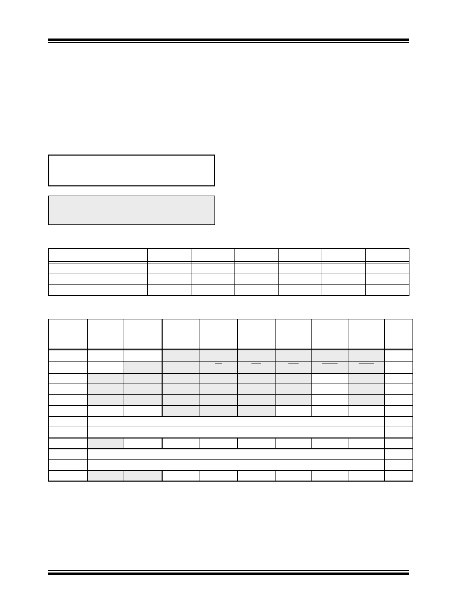
TABLE 13-3:
EXAMPLE PWM FREQUENCIES AND RESOLUTIONS AT 40 MHz
TABLE 13-4:
REGISTERS ASSOCIATED WITH PWM AND TIMER2
Note:
If the PWM duty cycle value is longer than
the PWM period, the CCP1 pin will not be
cleared.
FOSC
FPWM
---------------
log
2
()
log
-----------------------------bits
=
PWM Resolution (max)
PWM Frequency
2.44 kHz
9.77 kHz
39.06 kHz
156.25 kHz
312.50 kHz
416.67 kHz
Timer Prescaler (1, 4, 16)
16
41111
PR2 Value
FFh
3Fh
1Fh
17h
Maximum Resolution (bits)
10
8
7
6.58
Name
Bit 7
Bit 6
Bit 5
Bit 4
Bit 3
Bit 2
Bit 1
Bit 0
Reset
Values
on page
INTCON
GIE/GIEH PEIE/GIEL
TMR0IE
INT0IE
RBIE
TMR0IF
INT0IF
RBIF
RCON
IPEN
SBOREN(1)
—
RI
TO
PD
POR
BOR
PIR1
—
ADIF
RCIF
TXIF
—
CCP1IF
TMR2IF
TMR1IF
PIE1
—
ADIE
RCIE
TXIE
—
CCP1IE
TMR2IE
TMR1IE
IPR1
—
ADIP
RCIP
TXIP
—
CCP1IP
TMR2IP
TMR1IP
TRISC
TRISC7
TRISC6
—
TRISC2
TRISC1
TRISC0
TMR2
Timer2 Register
PR2
Timer2 Period Register
T2CON
—
T2OUTPS3 T2OUTPS2 T2OUTPS1 T2OUTPS0 TMR2ON
T2CKPS1
T2CKPS0
CCPR1L
Capture/Compare/PWM Register 1 Low Byte
CCPR1H
Capture/Compare/PWM Register 1 High Byte
CCP1CON
—
DC1B1
DC1B0
CCP1M3
CCP1M2
CCP1M1
CCP1M0
Legend: — = unimplemented, read as ‘0’. Shaded cells are not used by PWM or Timer2.
Note 1:
The SBOREN bit is only available when BOREN<1:0> = 01; otherwise, the bit reads as ‘0’.
相關PDF資料 |
PDF描述 |
|---|---|
| PIC16LF877T-04/PT | IC MCU FLASH 8KX14 EE A/D 44TQFP |
| PIC16LF877T-04/PQ | IC MCU FLASH 8KX14 EE A/D 44MQFP |
| PIC16LF871T-I/PT | IC MCU FLASH 2KX14 EE A/D 44TQFP |
| PIC16LF871T-I/L | IC MCU FLASH 2KX14 EE A/D 44PLCC |
| PIC16LF877T-04/L | IC MCU FLASH 8KX14 EE A/D 44PLCC |
相關代理商/技術參數(shù) |
參數(shù)描述 |
|---|---|
| PIC16LV923-04I/PT | 制造商:Microchip Technology Inc 功能描述: |
| PIC17C02-ME | 制造商:Microchip Technology Inc 功能描述:ELECTRONIC COMPONENT |
| PIC17C42/JW | 制造商:Microchip Technology Inc 功能描述: |
| PIC17C42-25/L | 制造商:Microchip Technology 功能描述:MCU 8-bit PIC17 PIC RISC 4KB EPROM 5V 44-Pin PLCC Tube |
| PIC17C4225L | 制造商:MICROCHIP 功能描述:New |
發(fā)布緊急采購,3分鐘左右您將得到回復。