- 您現(xiàn)在的位置:買賣IC網(wǎng) > PDF目錄368010 > PI74FCT163245 (Pericom Semiconductor Corp.) Fast CMOS 3.3V 16-Bit Bidirectional Transceiver PDF資料下載
參數(shù)資料
| 型號: | PI74FCT163245 |
| 廠商: | Pericom Semiconductor Corp. |
| 英文描述: | Fast CMOS 3.3V 16-Bit Bidirectional Transceiver |
| 中文描述: | 快速CMOS 3.3V的16位雙向收發(fā)器 |
| 文件頁數(shù): | 4/5頁 |
| 文件大?。?/td> | 57K |
| 代理商: | PI74FCT163245 |
PI74FCT163245
3.3V 16-BIT BIDIRECTIONAL TRANSCEIVER
4
PS2054B 01/18/99
12345678901234567890123456789012123456789012345678901234567890121234567890123456789012345678901212345678901234567890123456789012123456789012
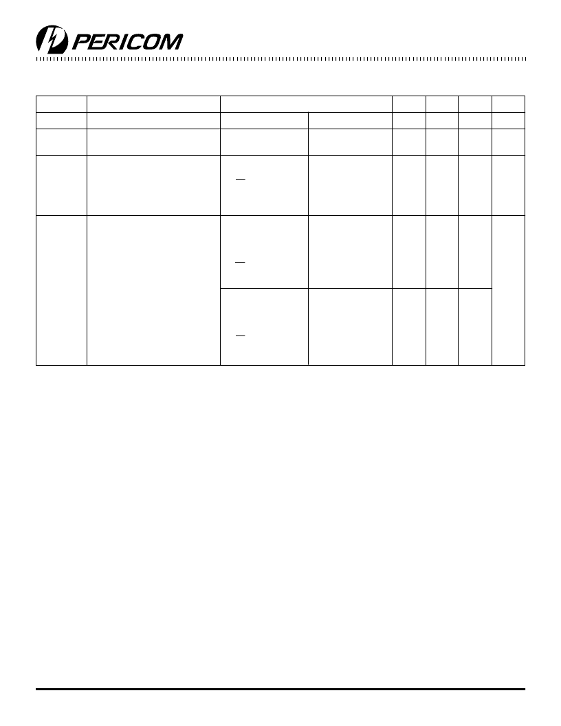
Power Supply Characteristics
Parameters Description
Test Conditions
(1)
Min.
Typ.
(2)
Max.
Units
I
CC
I
CC
Quiescent Power Supply Current
V
CC
= Max.
V
IN
= GND or V
CC
0.1
10
μA
Quiescent Power Supply Current
TTL Inputs HIGH
V
CC
= Max.
V
IN
= V
CC
– 0.6V
(3)
2.0
30
μA
I
CCD
Dynamic Power Supply
(4)
V
CC
= Max.,
Outputs Open
X
OE = xDIR = GND
One Bit Toggling
50% Duty Cycle
V
IN
= V
CC
V
IN
= GND
50
75
μA/
MHz
I
C
Total Power Supply
Current
(6)
V
CC
= Max.,
Outputs Open
f
I
= 10 MH
Z
50% Duty Cycle
X
OE = xDIR = GND
One Bit Toggling
V
IN
= V
CC
– 0.6V
V
IN
= GND
0.5
0.8
mA
V
CC
= Max.,
Outputs Open
f
I
= 2.5 MH
Z
50% Duty Cycle
X
OE = xDIR = GND
16 Bits Toggling
V
IN
= V
CC
– 0.6V
V
IN
= GND
2.0
3.3
(5)
Notes:
1. For Max. or Min. conditions, use appropriate value specified under Electrical Characteristics for the applicable device.
2. Typical values are at Vcc = 3.3V, +25°C ambient.
3. Per TTL driven input; all other inputs at Vcc or GND.
4. This parameter is not directly testable, but is derived for use in Total Power Supply Calculations.
5. Values for these conditions are examples of the Icc formula. These limits are guaranteed but not tested.
6. I
C
=I
QUIESCENT
+ I
INPUTS
+ I
DYNAMIC
I
C
= I
CC
+
I
CC
D
H
N
T
+ I
CCD
(f
CP
/2 + f
I
N
I
)
I
CC
= Quiescent Current (I
CCL
, I
CCH
and I
CCZ
)
I
CC
= Power Supply Current for a TTL High Input
D
H
= Duty Cycle for TTL Inputs High
N
T
= Number of TTL Inputs at D
H
I
CCD
= Dynamic Current Caused by an Input Transition Pair (HLH or LHL)
f
CP
= Clock Frequency for Register Devices (Zero for Non-Register Devices)
N
CP
= Number of Clock Inputs at f
CP
f
I
= Input Frequency
N
I
= Number of Inputs at f
I
All currents are in milliamps and all frequencies are in megahertz.
相關PDF資料 |
PDF描述 |
|---|---|
| PI74FCT163374 | Fast CMOS 3.3V 16-Bit Register (3-State) |
| PI74FCT2244ATH | Fast CMOS Octal Buffer/Line Drivers |
| PI74FCT244CTQ | Fast CMOS Octal Buffer/Line Drivers |
| PI74FCT244CTS | Fast CMOS Octal Buffer/Line Drivers |
| PI74FCT244DTQ | Fast CMOS Octal Buffer/Line Drivers |
相關代理商/技術參數(shù) |
參數(shù)描述 |
|---|---|
| PI74FCT163245A | 制造商:未知廠家 制造商全稱:未知廠家 功能描述:Dual 8-bit Bus Transceiver |
| PI74FCT163245AA | 制造商:Pericom Semiconductor Corporation 功能描述:Bus XCVR Dual 16-CH 3-ST 48-Pin TSSOP Tube |
| PI74FCT163245AK | 制造商:未知廠家 制造商全稱:未知廠家 功能描述:Dual 8-bit Bus Transceiver |
| PI74FCT163245ATA | 制造商:未知廠家 制造商全稱:未知廠家 功能描述:Dual 8-bit Bus Transceiver |
| PI74FCT163245ATV | 制造商:未知廠家 制造商全稱:未知廠家 功能描述:Dual 8-bit Bus Transceiver |
發(fā)布緊急采購,3分鐘左右您將得到回復。