- 您現(xiàn)在的位置:買賣IC網(wǎng) > PDF目錄368010 > PI74FCT163244 (Pericom Semiconductor Corp.) Fast CMOS 3.3V 16-Bit Buffer/Line Driver PDF資料下載
參數(shù)資料
| 型號: | PI74FCT163244 |
| 廠商: | Pericom Semiconductor Corp. |
| 英文描述: | Fast CMOS 3.3V 16-Bit Buffer/Line Driver |
| 中文描述: | 快速CMOS 3.3V的16位緩沖器/線路驅(qū)動器 |
| 文件頁數(shù): | 3/5頁 |
| 文件大?。?/td> | 163K |
| 代理商: | PI74FCT163244 |
PI74FCT163244
3.3V 16-BIT BUFFER/LINE DRIVER
3
12345678901234567890123456789012123456789012345678901234567890121234567890123456789012345678901212345678901234567890123456789012123456789012
12345678901234567890123456789012123456789012345678901234567890121234567890123456789012345678901212345678901234567890123456789012123456789012
PS2052B 01/18/99
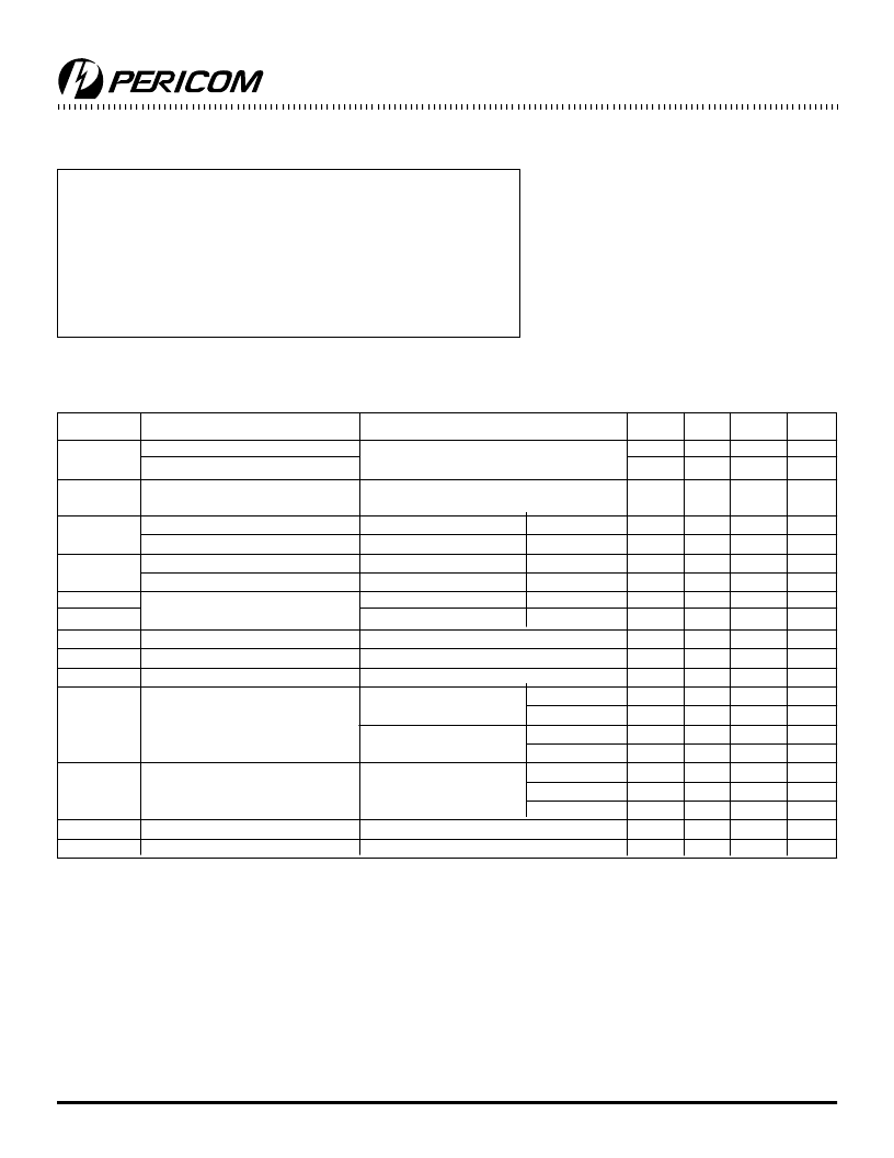
DC Electrical Characteristics
(Over the Operating Range, T
A
= –40°C to +85°C, V
CC
= 2.7V to 3.6V)
Parameters
V
IH
Description
Test Conditions
(1)
Min.
2.2
2.0
0.5
Typ
(2)
Max.
5.5
Vcc+0.5
0.8
Units
V
V
V
Input HIGH Voltage (Input pins)
Input HIGH Voltage (I/O pins)
Input LOW Voltage
(Input and I/O pins)
Input HIGH Current (Input pins)
Input HIGH Current (I/O pins)
Input LOW Current (Input pins)
Input LOW Current (I/O pins)
High Impedance Output Current
(3-State Output pins)
Clamp Diode Voltage
Output HIGH Current
Output LOW Current
Output HIGH Voltage
Guaranteed Logic HIGH Level
V
IL
Guaranteed Logic LOW Level
I
IH
V
CC
= Max.
V
CC
= Max.
V
CC
= Max.
V
CC
= Max.
V
CC
= Max.
V
CC
= Max.
V
CC
= Min., I
IN
= 18 mA
V
CC
= 3.3V, V
IN
= V
IH
or V
IL
, V
O
= 1.5V
(3)
36
V
CC
= 3.3V, V
IN
= V
IH
or V
IL
, V
O
= 1.5V
(3)
50
V
CC
= Min.
V
IN
= V
IH
or V
IL
V
CC
= 3.0V,
V
IN
= V
IH
OR
V
IL
V
CC
= Min.
V
IN
= V
IH
or V
IL
V
IN
= 5.5V
V
IN
= V
CC
V
IN
= GND
V
IN
= GND
V
OUT
= V
CC
V
OUT
= GND
0.7
60
90
3.0
3.0
0.2
0.3
85
150
±1
±1
±1
±1
±1
±1
1.2
110
200
0.2
0.4
0.5
240
μA
μA
μA
μA
μA
μA
V
mA
mA
V
V
V
V
V
V
V
mA
mV
I
IL
I
OZH
I
OZL
V
IK
I
ODH
I
ODL
V
OH
I
OH
= 0.1mA Vcc-0.2
I
OH
= 3mA
I
OH
= 8mA
I
OH
= 24mA
I
OL
= 0.1mA
I
OL
= 16mA
I
OL
= 24mA
2.4
2.4
(5)
2.0
60
V
OL
Output LOW Voltage
I
OS
V
H
Short Circuit Current
(4)
Input Hysteresis
V
CC
= Max.
(3)
, V
OUT
= GND
Storage Temperature .......................................................... 65°C to +150°C
Ambient Temperature with Power Applied ......................... 40°C to +85°C
Supply Voltage to Ground Potential (Inputs & Vcc Only)... 0.5V to +7.0V
Supply Voltage to Ground Potential (Outputs & D/O Only) 0.5V to +7.0V
DC Input Voltage .................................................................. 0.5V to +7.0V
DC Output Current ............................................................................ 120 mA
Power Dissipation ..................................................................................1.0W
Note:
Stresses greater than those listed under MAXIMUM
RATINGS may cause permanent damage to the de-
vice. This is a stress rating only and functional opera-
tion of the device at these or any other conditions
above those indicated in the operational sections of
this specification is not implied. Exposure to absolute
maximum rating conditions for extended periods may
affect reliability.
Notes:
1. For Max. or Min. conditions, use appropriate value specified under Electrical Characteristics for the applicable device type.
2. Typical values are at V
CC
= 3.3V, +25°C ambient and maximum loading.
3. Not more than one output should be shorted at one time. Duration of the test should not exceed one second.
4. This parameter is guaranteed but not tested.
5. V
OH
= V
CC
0.6V at rated current.
Maximum Ratings
(Above which the useful life may be impaired. For user guidelines, not tested.)
相關(guān)PDF資料 |
PDF描述 |
|---|---|
| PI74FCT163245 | Fast CMOS 3.3V 16-Bit Bidirectional Transceiver |
| PI74FCT163374 | Fast CMOS 3.3V 16-Bit Register (3-State) |
| PI74FCT2244ATH | Fast CMOS Octal Buffer/Line Drivers |
| PI74FCT244CTQ | Fast CMOS Octal Buffer/Line Drivers |
| PI74FCT244CTS | Fast CMOS Octal Buffer/Line Drivers |
相關(guān)代理商/技術(shù)參數(shù) |
參數(shù)描述 |
|---|---|
| PI74FCT163244A | 制造商:未知廠家 制造商全稱:未知廠家 功能描述:Quad 4-Bit Buffer/Driver |
| PI74FCT163244AA | 制造商:未知廠家 制造商全稱:未知廠家 功能描述:Quad 4-Bit Buffer/Driver |
| PI74FCT163244AK | 制造商:未知廠家 制造商全稱:未知廠家 功能描述:Quad 4-Bit Buffer/Driver |
| PI74FCT163244ATA | 制造商:未知廠家 制造商全稱:未知廠家 功能描述:Quad 4-Bit Buffer/Driver |
| PI74FCT163244ATV | 制造商:未知廠家 制造商全稱:未知廠家 功能描述:Quad 4-Bit Buffer/Driver |
發(fā)布緊急采購,3分鐘左右您將得到回復。