- 您現(xiàn)在的位置:買賣IC網(wǎng) > PDF目錄367952 > PI49FCT2805TS Five Distributed-Output Clock Driver PDF資料下載
參數(shù)資料
| 型號(hào): | PI49FCT2805TS |
| 英文描述: | Five Distributed-Output Clock Driver |
| 中文描述: | 五分布式輸出時(shí)鐘驅(qū)動(dòng)器 |
| 文件頁數(shù): | 3/5頁 |
| 文件大?。?/td> | 242K |
| 代理商: | PI49FCT2805TS |
PI49FCT807/2807T
Fast CMOS Clock Driver
3
PS7008B 02/17/99
12345678901234567890123456789012123456789012345678901234567890121234567890123456789012345678901212345678901234567890123456789012123456789012
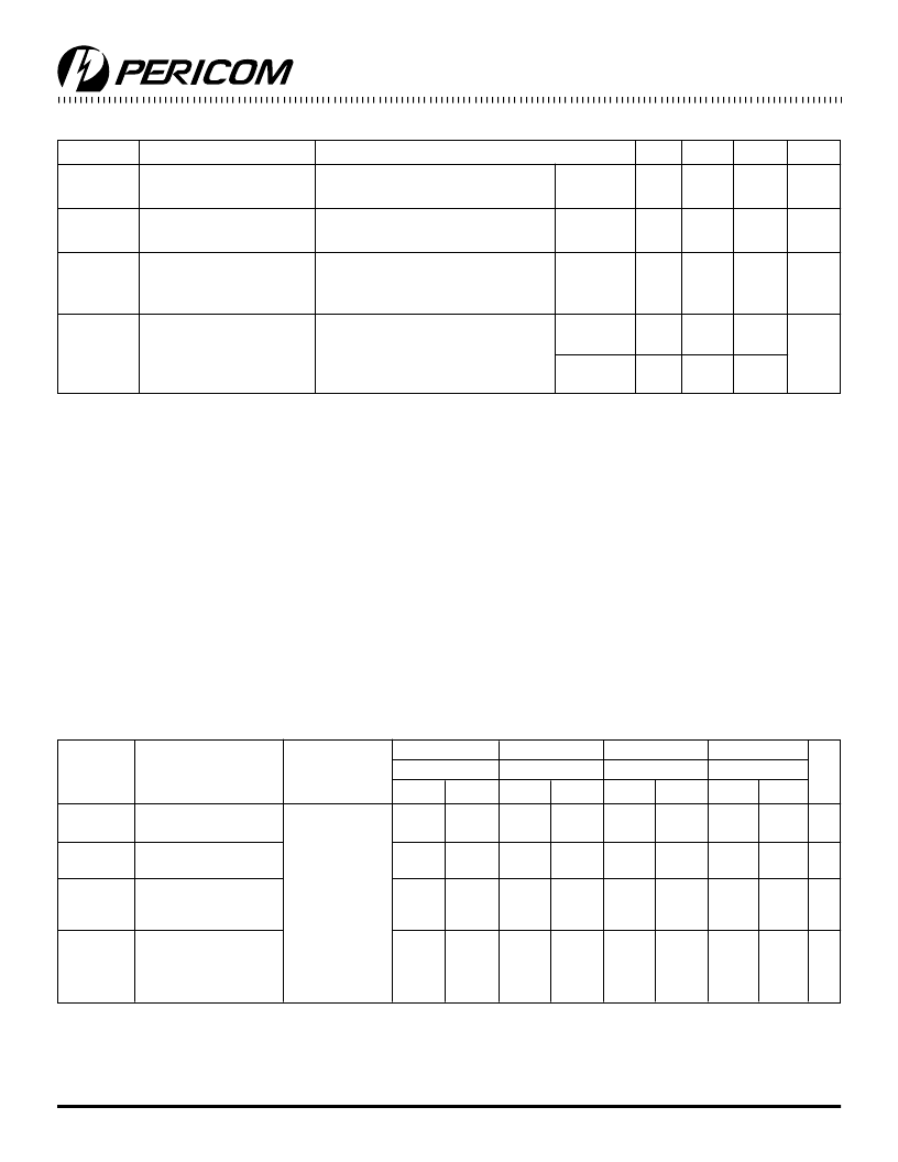
Power Supply Characteristics
Parameters Description
Test Conditions
(1)
Min.
Typ.
(2)
Max.
Units
I
CC
Quiescent Power
Supply Current
V
CC
= Max.
V
IN
= GND
or Vcc
3
30
μA
I
CC
Supply Current per
Input @ TTL HIGH
V
CC
= Max.,
V
IN
=
3.4V
(3)
0.5
1.5
mA
I
CCD
Supply Current per
Input per MHz
(4)
V
CC
= Max., Outputs Open
50% Duty Cycle,
One Input Toggling
V
IN
= V
CC
V
IN
= GND
0.4
0.6
mA/
MHz
I
C
Total Power Supply
Current
(6)
V
CC
= Max., Outputs Open
f
CP
= 50 MH
Z
,
50% Duty Cycle
V
IN
= V
CC
V
IN
= GND
V
IN
= 3.4V
V
IN
= GND
20
30
(5)
mA
20.7
33
(5)
Notes:
1. For Max. or Min. conditions, use appropriate value specified under Electrical Characteristics for the applicable device.
2. Typical values are at Vcc = 5.0V, +25°C ambient.
3. Per TTL driven input (V
IN
= 3.4V); all other inputs at Vcc or GND.
4. This parameter is not directly testable, but is derived for use in Total Power Supply Calculations.
5. Values for these conditions are examples of the Icc formula. These limits are guaranteed but not tested.
6. I
C
=I
QUIESCENT
+ I
INPUTS
+ I
DYNAMIC
I
C
= I
CC
+
I
CC
D
H
N
T
+ I
CCD
(f
CP
/2 + f
I
N
I
)
I
CC
= Quiescent Current
I
CC
= Power Supply Current for a TTL High Input (V
IN
= 3.4V)
D
H
= Duty Cycle for TTL Inputs High
N
T
= Number of TTL Inputs at D
H
I
CCD
= Dynamic Current Caused by an Input Transition Pair (HLH or LHL)
f
CP
= Clock Frequency for Register Devices (Zero for Non-Register Devices)
f
I
= Input Frequency
N
I
= Number of Inputs at f
I
All currents are in milliamps and all frequencies are in megahertz.
Switching Characteristics over Operating Range
807/2807T
807AT
807BT
807CT
Com.
Com.
Com.
Com.
Parameters
Description
Conditions
(1)
Min.
Max.
Min.
Max.
Min.
Max.
Min.
Max.
Units
t
PLH
t
PHL
t
SK(o)
Propagation Delay
A
TO
B
N
Skew between two outputs
of same package
(3)
Skew between opposite
transitions of same
output (|t
PHL
— t
PLH
|)
(3)
Skew between outputs of
different package at same
power supply, temperature
and speed grade
(3)
C
L
= 50pF
R
L
= 500
1.5
4.5
1.5
4.0
1.5
3.8
1.5
3.5
ns
—
0.5
—
0.5
—
0.35
—
0.25
ns
t
SK(p)
—
0.5
—
0.5
—
0.35
—
0.35
ns
t
SK(t)
—
1.0
—
1.0
—
0.75
—
0.75
ns
Notes:
1. See test circuit and wave forms.
2. Minimum limits are guaranteed but not tested on Propagation Delays.
3. This parameter is guaranteed but not tested.
相關(guān)PDF資料 |
PDF描述 |
|---|---|
| PI49FCT2807ATH | Low Power, 14-Bit, 200ksps ADC with Serial and Parallel I/O; Package: SSOP; No of Pins: 28; Temperature Range: -40°C to +85°C |
| PI49FCT2807ATP | Ten Distributed-Output Clock Driver |
| PI49FCT2807ATQ | Ten Distributed-Output Clock Driver |
| PI49FCT2807ATS | 14-Bit, 800ksps Sampling A/D Converter with Shutdown; Package: SSOP; No of Pins: 28; Temperature Range: 0°C to +70°C |
| PI49FCT2807BTH | 14-Bit, 800ksps Sampling A/D Converter with Shutdown; Package: SO; No of Pins: 28; Temperature Range: 0°C to +70°C |
相關(guān)代理商/技術(shù)參數(shù) |
參數(shù)描述 |
|---|---|
| PI49FCT2805TSA | 制造商:PERICOM 制造商全稱:Pericom Semiconductor Corporation 功能描述:Fast CMOS Buffer/Clock Driver |
| PI49FCT2805TSB | 制造商:PERICOM 制造商全稱:Pericom Semiconductor Corporation 功能描述:Fast CMOS Buffer/Clock Driver |
| PI49FCT2805TSC | 制造商:PERICOM 制造商全稱:Pericom Semiconductor Corporation 功能描述:Fast CMOS Buffer/Clock Driver |
| PI49FCT2805TSE | 功能描述:時(shí)鐘緩沖器 Non Inverting Clock Driver RoHS:否 制造商:Texas Instruments 輸出端數(shù)量:5 最大輸入頻率:40 MHz 傳播延遲(最大值): 電源電壓-最大:3.45 V 電源電壓-最小:2.375 V 最大功率耗散: 最大工作溫度:+ 85 C 最小工作溫度:- 40 C 封裝 / 箱體:LLP-24 封裝:Reel |
| PI49FCT2805TSEX | 功能描述:時(shí)鐘緩沖器 Non Inverting Clock Driver RoHS:否 制造商:Texas Instruments 輸出端數(shù)量:5 最大輸入頻率:40 MHz 傳播延遲(最大值): 電源電壓-最大:3.45 V 電源電壓-最小:2.375 V 最大功率耗散: 最大工作溫度:+ 85 C 最小工作溫度:- 40 C 封裝 / 箱體:LLP-24 封裝:Reel |
發(fā)布緊急采購,3分鐘左右您將得到回復(fù)。