- 您現(xiàn)在的位置:買賣IC網(wǎng) > PDF目錄367938 > PHP55N03LT (NXP SEMICONDUCTORS) N-channel TrenchMOS transistor Logic level FET(N溝道TrenchMOS 晶體管邏輯電平場效應(yīng)管) PDF資料下載
參數(shù)資料
| 型號: | PHP55N03LT |
| 廠商: | NXP SEMICONDUCTORS |
| 元件分類: | JFETs |
| 英文描述: | N-channel TrenchMOS transistor Logic level FET(N溝道TrenchMOS 晶體管邏輯電平場效應(yīng)管) |
| 中文描述: | 55 A, 25 V, 0.018 ohm, N-CHANNEL, Si, POWER, MOSFET, TO-220AB |
| 封裝: | PLASTIC, TO-220AB, 3 PIN |
| 文件頁數(shù): | 1/11頁 |
| 文件大小: | 107K |
| 代理商: | PHP55N03LT |
Philips Semiconductors
Product specification
N-channel TrenchMOS
transistor
Logic level FET
PHP55N03LT, PHB55N03LT
PHD55N03LT
FEATURES
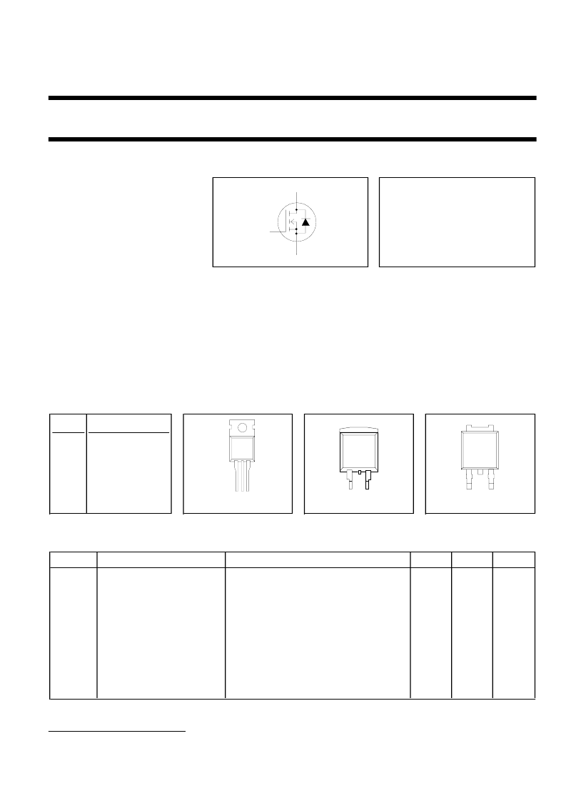
SYMBOL
QUICK REFERENCE DATA
V
DSS
= 25 V
’Trench’
technology
Very low on-state resistance
Fast switching
Low thermal resistance
Logic level compatible
I
D
= 55 A
R
DS(ON)
≤
14 m
(V
GS
= 10 V)
R
DS(ON)
≤
18 m
(V
GS
= 5 V)
GENERAL DESCRIPTION
N-channel enhancement mode logic level field-effect power transistor in a plastic envelope using ’
trench
’ technology.
Applications:-
High frequency computer motherboard d.c. to d.c. converters
High current switching
The PHP55N03LT is supplied in the SOT78 (TO220AB) conventional leaded package.
The PHB55N03LT is supplied in the SOT404 (D
2
PAK) surface mounting package.
The PHD55N03LT is supplied in the SOT428 (DPAK)surface mounting package.
PINNING
SOT78 (TO220AB)
SOT404 (D
2
PAK)
SOT428 (DPAK)
PIN
DESCRIPTION
1
gate
2
drain
1
3
source
tab
drain
LIMITING VALUES
Limiting values in accordance with the Absolute Maximum System (IEC 134)
SYMBOL PARAMETER
V
DSS
Drain-source voltage
V
DGR
Drain-gate voltage
V
GS
Gate-source voltage (DC)
V
GSM
Gate-source voltage (pulse
peak value)
I
D
Drain current (DC)
CONDITIONS
T
j
= 25 C to 175C
T
j
= 25 C to 175C; R
GS
= 20 k
MIN.
-
-
-
-
MAX.
25
25
±
15
±
20
UNIT
V
V
V
V
T
j
≤
150C
T
mb
= 25 C
T
mb
= 100 C
T
mb
= 25 C
-
-
-
55
38
220
A
A
A
I
DM
Drain current (pulse peak
value)
Total power dissipation
Operating junction and
storage temperature
P
tot
T
j
, T
stg
T
mb
= 25 C
-
103
175
W
C
- 55
d
g
s
1 2 3
tab
1
3
tab
2
1
2
3
tab
1
It is not possible to make connection to pin:2 of the SOT404 or SOT428 packages.
October 1999
1
Rev 1.200
相關(guān)PDF資料 |
PDF描述 |
|---|---|
| PHB69N03LT | N-channel TrenchMOS transistor Logic level FET(N溝道TrenchMOS 晶體管邏輯電平場效應(yīng)管) |
| PHD69N03LT | N-channel TrenchMOS transistor Logic level FET(N溝道TrenchMOS 晶體管邏輯電平場效應(yīng)管) |
| PHP69N03LT | N-channel TrenchMOS transistor Logic level FET(N溝道TrenchMOS 晶體管邏輯電平場效應(yīng)管) |
| PHB69N03T | TrenchMOS transistor Standard Level FET(TrenchMOS 晶體管標(biāo)準(zhǔn)電平場效應(yīng)管) |
| PHB80N06LT | TrenchMOS transistor Logic level FET |
相關(guān)代理商/技術(shù)參數(shù) |
參數(shù)描述 |
|---|---|
| PHP55N03LTA | 制造商:PHILIPS 制造商全稱:NXP Semiconductors 功能描述:N-channel enhancement mode field-effect transistor |
| PHP55N03LTA,127 | 功能描述:MOSFET RAIL PWR-MOS RoHS:否 制造商:STMicroelectronics 晶體管極性:N-Channel 汲極/源極擊穿電壓:650 V 閘/源擊穿電壓:25 V 漏極連續(xù)電流:130 A 電阻汲極/源極 RDS(導(dǎo)通):0.014 Ohms 配置:Single 最大工作溫度: 安裝風(fēng)格:Through Hole 封裝 / 箱體:Max247 封裝:Tube |
| PHP55N03T | 制造商:PHILIPS 制造商全稱:NXP Semiconductors 功能描述:TrenchMOS transistor Standard level FET |
| PHP55N04LT | 制造商:未知廠家 制造商全稱:未知廠家 功能描述:TRANSISTOR | MOSFET | N-CHANNEL | 35V V(BR)DSS | 55A I(D) | TO-220AB |
| PHP5N20E | 制造商:DANAHER - INDUSTRIAL/SPECIALTY 功能描述:LS-7 316 Stainless Steel, Polypropylene, TFE, .55 Sp. Gr, 100 PSI @ 70 F |
發(fā)布緊急采購,3分鐘左右您將得到回復(fù)。