- 您現(xiàn)在的位置:買(mǎi)賣(mài)IC網(wǎng) > PDF目錄367928 > PGA202 Precision Instrumentation Amplifier PDF資料下載
參數(shù)資料
| 型號(hào): | PGA202 |
| 元件分類(lèi): | 測(cè)量放大器 |
| 英文描述: | Precision Instrumentation Amplifier |
| 中文描述: | 精密儀表放大器 |
| 文件頁(yè)數(shù): | 8/10頁(yè) |
| 文件大小: | 139K |
| 代理商: | PGA202 |
PGA202/203
8
GAIN SELECTION
Gain selection is accomplished by the application of a 2-bit
digital word to the gain select inputs. Table I shows the gains
for the different possible values of the digital input word.
The logic inputs are referred to their own separate digital
common pin, which can be connected to any voltage be-
tween the minus supply and 8V below the positive supply.
The gains are all internally trimmed to an initial accuracy of
better than 0.1%, so no external gain adjustment is required.
However, if necessary the gains can be increased by the use
of an external attenuator around the output stage as shown in
Figure 3. Recommended resistor values for certain selected
output gains are given in Table II.
PGA202
PGA203
A
1
A
0
GAIN
ERROR
GAIN
ERROR
0
0
1
1
0
1
0
1
1
10
100
1000
0.05%
0.05%
0.05%
0.10%
1
2
4
8
0.05%
0.05%
0.05%
0.05%
TABLE I. Software Gain Selection.
TABLE II. Output Stage Gain Control.
OUTPUT GAIN
R
1
5k
2k
1k
R
2
5k
8k
9k
2
5
10
FIGURE 3. Gain Increase with Buffered Attenuator.
COMMON-MODE INPUT RANGE
Unlike the classical three op amp type of circuit, the input
common-mode range of the PGA202/203 does not depend
on the differential input and the gain. In the standard three
op amp circuit, the input common-mode signal must be kept
below the maximum output voltage of the input amplifier
minus 1/2 the final output voltage. If, for example, these
amplifiers can swing
±
12V, then to get 12V at the output you
must restrict the input common-mode voltage to only 6V.
The circuitry of the PGA202/203 is such that the common-
mode input range applies to either input pin regardless of the
output voltage.
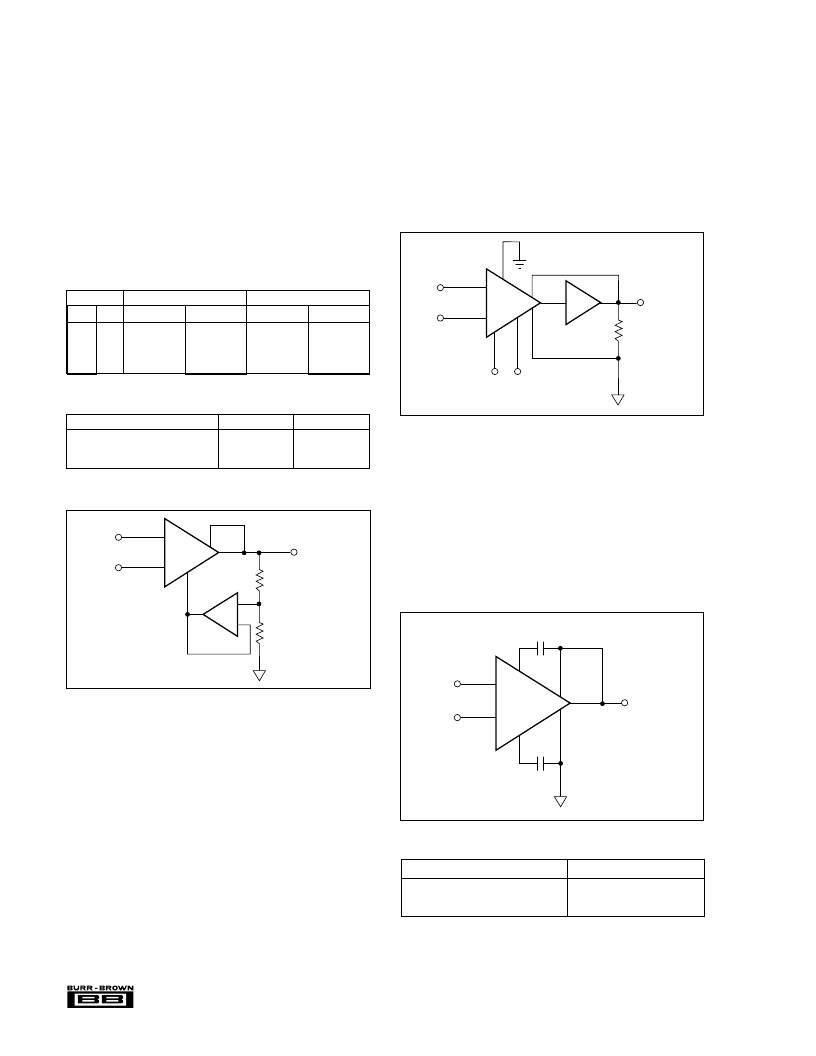
FIGURE 4. Current Boosting the Output.
OUTPUT SENSE
An output sense has been provided to allow greater accuracy
in connecting the load. By attaching this feedback point to
the load at the load site, IR drops due to the load currents are
eliminated since they are inside the feedback loop. Proper
connection is shown in Figure 1. When more current is
required, a power booster can be placed in the feedback loop
as shown in Figure 4. Buffer errors are minimized by the
loop gain of the output amplifier.
OUTPUT FILTERING
The summing nodes of the output amplifier have also been
made available to allow for output filtering. By placing
matched capacitors in parallel with the existing internal
capacitors as shown in Figure 5, you can lower the fre-
quency response of the output amplifier. This will reduce the
noise of the amplifier, at the cost of a slower response. The
nominal frequency responses for some selected values of
capacitor are shown in Table III.
FIGURE 5. Output Filtering.
CUTOFF FREQUENCY
C
1
AND C
2
1MHz
100kHz
10kHz
None
47pF
525pF
TABLE III. Output Frequency vs Filter Capacitors.
PGA202
8
7
2
1112
+
–
V
OUT
OPA633
V
IN
1
14
4
R
L
A
0
A
1
PGA202
8
7
4
1112
+
–
V
OUT
+
–
V
IN
R
1
R
2
OPA602
PGA202
8
7
10
4
1112
V
OUT
+
–
V
IN
5
C
EXT
C
EXT
相關(guān)PDF資料 |
PDF描述 |
|---|---|
| PGA202AG | Precision Instrumentation Amplifier |
| PGA202BG | Precision Instrumentation Amplifier |
| PGA202KP | Precision Instrumentation Amplifier |
| PGA203 | Precision Instrumentation Amplifier |
| PGA203AG | Precision Instrumentation Amplifier |
相關(guān)代理商/技術(shù)參數(shù) |
參數(shù)描述 |
|---|---|
| PGA202/PGA203 | 制造商:BB 制造商全稱(chēng):BB 功能描述:PGA202. PGA203 - Digitally Controlled Programmable-Gain INSTRUMENTATION AMPLIFIER |
| PGA202AG | 制造商:BB 制造商全稱(chēng):BB 功能描述:Digitally Controlled Programmable-Gain INSTRUMENTATION AMPLIFIER |
| PGA202BG | 制造商:BB 制造商全稱(chēng):BB 功能描述:Digitally Controlled Programmable-Gain INSTRUMENTATION AMPLIFIER |
| PGA202KP | 功能描述:儀表放大器 Digitally Controlled Programmable-Gain RoHS:否 制造商:Texas Instruments 通道數(shù)量: 輸入補(bǔ)償電壓:150 V 可用增益調(diào)整: 最大輸入電阻:10 kOhms 共模抑制比(最小值):88 dB 工作電源電壓:2.7 V to 36 V 電源電流:200 uA 最大工作溫度:+ 125 C 最小工作溫度:- 40 C 封裝 / 箱體:MSOP-8 封裝:Bulk |
| PGA202KP | 制造商:BURR-BROWN 功能描述:AMP INSTRUMENT PROG GAIN DIP 202 |
發(fā)布緊急采購(gòu),3分鐘左右您將得到回復(fù)。