- 您現(xiàn)在的位置:買賣IC網 > PDF目錄367911 > PFB6000 (Electronic Theatre Controls, Inc.) N-CHANNEL TRENCH MOSFET PDF資料下載
參數資料
| 型號: | PFB6000 |
| 廠商: | Electronic Theatre Controls, Inc. |
| 英文描述: | N-CHANNEL TRENCH MOSFET |
| 中文描述: | N溝道溝道MOSFET |
| 文件頁數: | 2/3頁 |
| 文件大?。?/td> | 136K |
| 代理商: | PFB6000 |
PFB6000
N-C
HANNEL
T
RENCH
M
OSFET
2004/03/04
Page 2
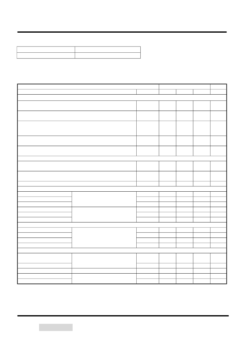
ORDERING INFORMATION
Part Number
PFB6000
ELECTRICAL CHARACTERISTICS
Unless otherwise specified, T
J
= 25
Package
TO-220
.
CMP60N03LD13
Typ
Characteristic
Symbol
Min
Max
Units
OFF Characteristics
Drain-to-Source Breakdown Voltage
(V
GS
= 0 V, I
D
= 250
Breakdown Voltage Temperature Coefficient
(Reference to 25
,
I
D
= 250
Drain-to-Source Leakage Current
(V
DS
= 60 V, V
GS
= 0 V, T
J
= 25
(V
DS
= 48 V, V
GS
= 0 V, T
J
= 150
Gate-to-Source Forward Leakage
(V
GS
= 20 V)
Gate-to-Source Reverse Leakage
(V
GS
= -20 V)
A)
V
DSS
60
V
A)
V
DSS
/
T
J
0.069
mV/
)
)
I
DSS
25
250
100
μA
I
GSS
nA
I
GSS
-100
nA
ON Characteristics
Gate Threshold Voltage
(V
DS
= V
GS
, I
D
= 250
Static Drain-to-Source On-Resistance (Note 4)
(V
GS
= 10 V, I
D
= 60A)
Forward Transconductance (V
DS
= 15 V, I
D
= 60A) (Note 4)
A)
V
GS(th)
1.0
2.0
3.0
V
R
DS(on)
15.8
36
18
m
g
FS
S
Dynamic Characteristics
Input Capacitance
Output Capacitance
Reverse Transfer Capacitance
Total Gate Charge (V
GS
= 10 V)
Gate-to-Source Charge
Gate-to-Drain (“Miller”) Charge
C
iss
C
oss
C
rss
Q
g
Q
gs
Q
gd
1430
420
88
37.7
8.4
9.8
pF
pF
pF
(V
DS
= 25 V, V
GS
= 0 V,
f = 1.0 MHz)
nC
nC
nC
(V
DS
= 30 V, I
D
= 60 A,
V
GS
= 10 V) (Note 5)
Resistive Switching Characteristics
Turn-On Delay Time
Rise Time
Turn-Off Delay Time
Fall Time
t
d(on)
t
rise
t
d(off)
t
fall
12.1
64
69
39
ns
ns
ns
ns
(V
DD
= 30 V, I
D
= 60 A,
V
GS
= 10 V,
R
G
= 9.1
) (Note 5)
Source-Drain Diode Characteristics
Continuous Source Current
(Body Diode)
Pulse Source Current (Body Diode)
Diode Forward On-Voltage
Reverse Recovery Time
Reverse Recovery Charge
I
S
60
A
Integral pn-diode in MOSFET
I
SM
V
SD
t
rr
Q
rr
241
1.5
A
V
ns
nC
(I
S
= 60 A, V
GS
= 0 V)
(I
F
= 60A, V
GS
= 0 V,
d
i
/d
t
= 100A/μs)
55
110
相關PDF資料 |
PDF描述 |
|---|---|
| PFC375-4002F | PSU 350 W 4 O/P |
| PFC375-1024F | PSU 375W 2 O/P 24V |
| PFC375-1048F | PSU 375W 48V |
| PFC375-3001F | PSU 375W 3 O/P |
| PFC375-4000F | PSU 350 WATT 4 O/P |
相關代理商/技術參數 |
參數描述 |
|---|---|
| PFB63 | 制造商:ROEBUCK 功能描述:RBK HT SET BZP M8X50 (PK 200) |
| PFB66 | 制造商:ROEBUCK 功能描述:RBK HT SET BZP M10X30 (PK 200) |
| PFB68 | 制造商:ROEBUCK 功能描述:RBK HT SET BZP M10X40 (PK 100) |
| PFB69 | 制造商:ROEBUCK 功能描述:RBK HT SET BZP M12X30 (PK 100) |
| PFB6M | 制造商:Panduit Corp 功能描述:CONDUIT CLIP FOR 3/8 CONDUIT WITH ANGLE |
發(fā)布緊急采購,3分鐘左右您將得到回復。