PCA9554_9554A
All information provided in this document is subject to legal disclaimers.
NXP B.V. 2013. All rights reserved.
Product data sheet
Rev. 9 — 19 March 2013
12 of 35
NXP Semiconductors
PCA9554; PCA9554A
8-bit I2C-bus and SMBus I/O port with interrupt
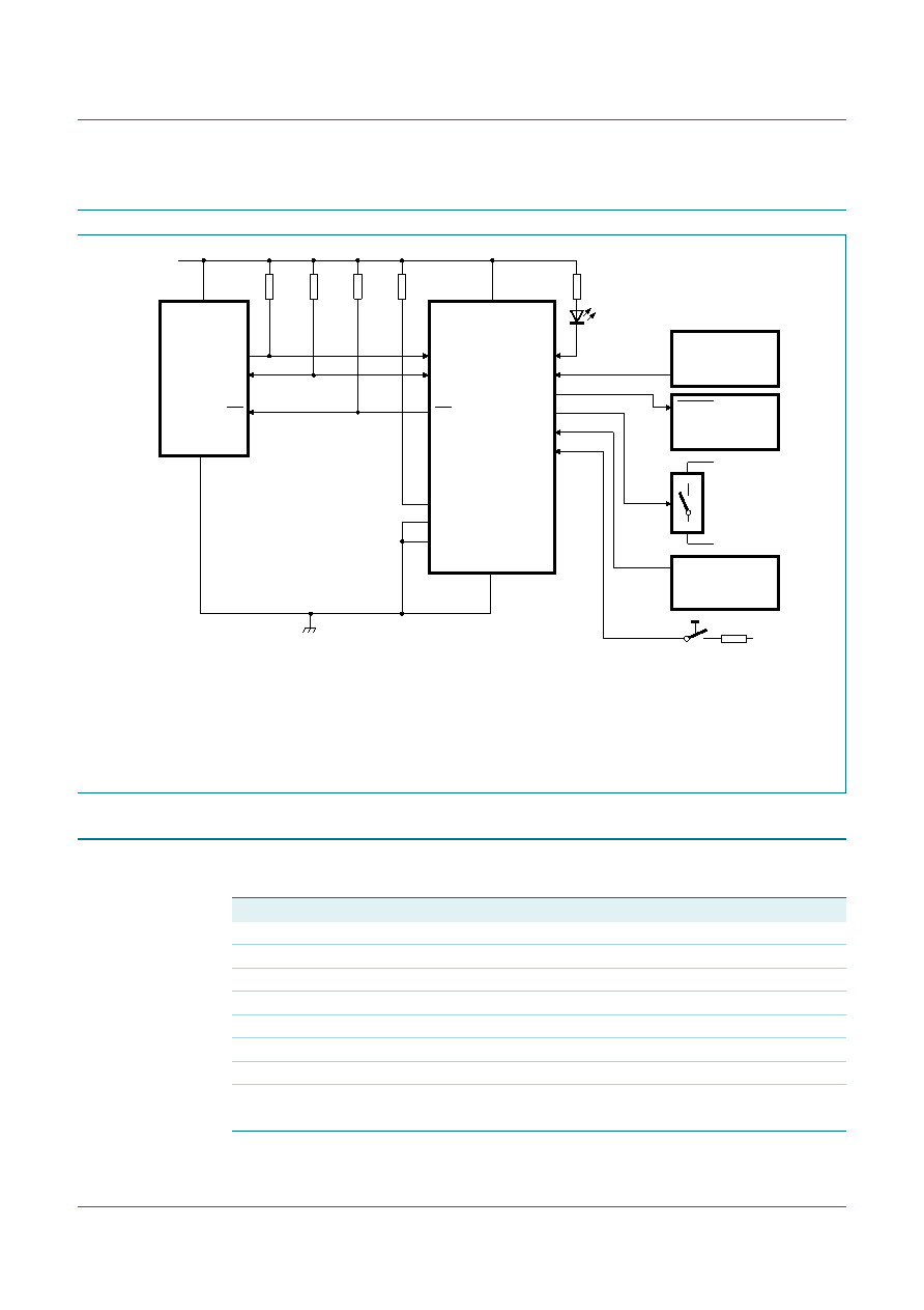
7.
Application design-in information
8.
Limiting values
Device address configured as 0100 100X for this example.
IO0, IO1, IO2 configured as outputs.
IO3, IO4, IO5 configured as inputs.
IO6 and IO7 are not used and must be configured as outputs.
Fig 15. Typical application
PCA9554
IO0
IO1
SCL
SDA
VDD
002aac496
SCL
SDA
IO2
IO3
VDD
VSS
MASTER
CONTROLLER
VSS
VDD (5 V)
2 k
Ω
SUBSYSTEM 1
(e.g., temp. sensor)
INT
SUBSYSTEM 2
(e.g., counter)
RESET
controlled switch
(e.g., CBT device)
A
B
enable
INT
10 k
Ω
10 k
Ω
SUBSYSTEM 3
(e.g., alarm system)
ALARM
IO4
IO5
VDD
A2
A1
A0
IO6
IO7
10 k
Ω
10 k
Ω
Table 9.
Limiting values
In accordance with the Absolute Maximum Rating System (IEC 60134).
Symbol
Parameter
Conditions
Min
Max
Unit
VDD
supply voltage
0.5
+6.0
V
II
input current
-
20
mA
VI/O
voltage on an input/output pin
VSS 0.5
5.5
V
IO(IOn)
output current on pin IOn
-
50
mA
IDD
supply current
-
85
mA
ISS
ground supply current
-
100
mA
Ptot
total power dissipation
-
200
mW
Tstg
storage temperature
65
+150
C
Tamb
ambient temperature
operating
40
+85
C
