- 您現(xiàn)在的位置:買(mǎi)賣(mài)IC網(wǎng) > PDF目錄367740 > P89C51RB2HFP (NXP SEMICONDUCTORS) 80C51 8-bit Flash microcontroller family 16KB/32KB/64KB ISP/IAP Flash with 512B/512B/1KB RAM PDF資料下載
參數(shù)資料
| 型號(hào): | P89C51RB2HFP |
| 廠(chǎng)商: | NXP SEMICONDUCTORS |
| 元件分類(lèi): | 微控制器/微處理器 |
| 英文描述: | 80C51 8-bit Flash microcontroller family 16KB/32KB/64KB ISP/IAP Flash with 512B/512B/1KB RAM |
| 中文描述: | 8-BIT, FLASH, 33 MHz, MICROCONTROLLER, PDIP40 |
| 封裝: | 0.600 INCH, PLASTIC, SOT-129-1, DIP-40 |
| 文件頁(yè)數(shù): | 6/52頁(yè) |
| 文件大小: | 289K |
| 代理商: | P89C51RB2HFP |
第1頁(yè)第2頁(yè)第3頁(yè)第4頁(yè)第5頁(yè)當(dāng)前第6頁(yè)第7頁(yè)第8頁(yè)第9頁(yè)第10頁(yè)第11頁(yè)第12頁(yè)第13頁(yè)第14頁(yè)第15頁(yè)第16頁(yè)第17頁(yè)第18頁(yè)第19頁(yè)第20頁(yè)第21頁(yè)第22頁(yè)第23頁(yè)第24頁(yè)第25頁(yè)第26頁(yè)第27頁(yè)第28頁(yè)第29頁(yè)第30頁(yè)第31頁(yè)第32頁(yè)第33頁(yè)第34頁(yè)第35頁(yè)第36頁(yè)第37頁(yè)第38頁(yè)第39頁(yè)第40頁(yè)第41頁(yè)第42頁(yè)第43頁(yè)第44頁(yè)第45頁(yè)第46頁(yè)第47頁(yè)第48頁(yè)第49頁(yè)第50頁(yè)第51頁(yè)第52頁(yè)
Philips Semiconductors
Preliminary specification
89C51RB2/89C51RC2/
89C51RD2
80C51 8-bit Flash microcontroller family
16KB/32KB/64KB ISP/IAP Flash with 512B/512B/1KB RAM
1999 Sep 23
6
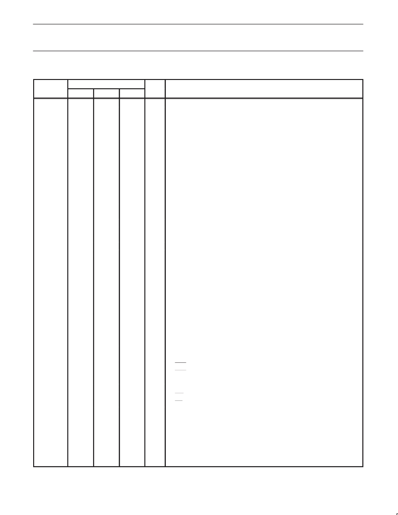
PIN DESCRIPTIONS
MNEMONIC
PIN NUMBER
TYPE
NAME AND FUNCTION
PDIP
PLCC
PQFP
V
SS
V
CC
20
22
16
I
Ground:
0 V reference.
40
44
38
I
Power Supply:
This is the power supply voltage for normal, idle, and power-down
operation.
P0.0–0.7
39–32
43–36
37–30
I/O
Port 0:
Port 0 is an open-drain, bidirectional I/O port. Port 0 pins that have 1s
written to them float and can be used as high-impedance inputs. Port 0 is also the
multiplexed low-order address and data bus during accesses to external program
and data memory. In this application, it uses strong internal pull-ups when emitting 1s.
P1.0–P1.7
1–8
2–9
40–44,
1–3
I/O
Port 1:
Port 1 is an 8-bit bidirectional I/O port with internal pull-ups on all pins
except P1.6 and P1.7 which are open drain. Port 1 pins that have 1s written to them
are pulled high by the internal pull-ups and can be used as inputs. As inputs, port 1
pins that are externally pulled low will source current because of the internal
pull-ups. (See DC Electrical Characteristics: I
IL
).
Alternate functions for 89C51RB2/RC2/RD2 Port 1 include:
T2 (P1.0):
Timer/Counter 2 external count input/Clockout (see Programmable
Clock-Out)
T2EX (P1.1):
Timer/Counter 2 Reload/Capture/Direction Control
ECI (P1.2):
External Clock Input to the PCA
CEX0 (P1.3):
Capture/Compare External I/O for PCA module 0
CEX1 (P1.4):
Capture/Compare External I/O for PCA module 1
CEX2 (P1.5):
Capture/Compare External I/O for PCA module 2
CEX3 (P1.6):
Capture/Compare External I/O for PCA module 3
CEX4 (P1.7):
Capture/Compare External I/O for PCA module 4
1
2
40
I/O
2
3
4
5
6
7
8
3
4
5
6
7
8
9
41
42
43
44
1
2
3
I
I
I/O
I/O
I/O
I/O
I/O
P2.0–P2.7
21–28
24–31
18–25
I/O
Port 2:
Port 2 is an 8-bit bidirectional I/O port with internal pull-ups. Port 2 pins that
have 1s written to them are pulled high by the internal pull-ups and can be used as
inputs. As inputs, port 2 pins that are externally being pulled low will source current
because of the internal pull-ups. (See DC Electrical Characteristics: I
IL
). Port 2
emits the high-order address byte during fetches from external program memory
and during accesses to external data memory that use 16-bit addresses (MOVX
@DPTR). In this application, it uses strong internal pull-ups when emitting 1s.
During accesses to external data memory that use 8-bit addresses (MOV @Ri),
port 2 emits the contents of the P2 special function register.
P3.0–P3.7
10–17
11,
13–19
5, 7–13
I/O
Port 3:
Port 3 is an 8-bit bidirectional I/O port with internal pull-ups. Port 3 pins that
have 1s written to them are pulled high by the internal pull-ups and can be used as
inputs. As inputs, port 3 pins that are externally being pulled low will source current
because of the pull-ups. (See DC Electrical Characteristics: I
). Port 3 also serves
the special features of the 89C51RB2/RC2/RD2, as listed below:
RxD (P3.0):
Serial input port
TxD (P3.1):
Serial output port
INT0 (P3.2):
External interrupt
INT1 (P3.3):
External interrupt
T0 (P3.4):
Timer 0 external input
T1 (P3.5):
Timer 1 external input
WR (P3.6):
External data memory write strobe
RD (P3.7):
External data memory read strobe
10
11
12
13
14
15
16
17
11
13
14
15
16
17
18
19
5
7
8
9
10
11
12
13
I
O
I
I
I
I
O
O
RST
9
10
4
I
Reset:
A high on this pin for two machine cycles while the oscillator is running,
resets the device. An internal diffused resistor to V
SS
permits a power-on reset
using only an external capacitor to V
CC
.
Address Latch Enable:
Output pulse for latching the low byte of the address
during an access to external memory. In normal operation, ALE is emitted twice
every machine cycle, and can be used for external timing or clocking. Note that one
ALE pulse is skipped during each access to external data memory. ALE can be
disabled by setting SFR auxiliary.0. With this bit set, ALE will be active only during a
MOVX instruction.
ALE
30
33
27
O
相關(guān)PDF資料 |
PDF描述 |
|---|---|
| P89C51RC2FA | 80C51 8-bit Flash microcontroller family 16KB/32KB/64KB ISP/IAP Flash with 512B/512B/1KB RAM |
| P89C51RC2FB | 80C51 8-bit Flash microcontroller family 16KB/32KB/64KB ISP/IAP Flash with 512B/512B/1KB RAM |
| P89C51RD2BB | 80C51 8-bit Flash microcontroller family 16KB/32KB/64KB ISP/IAP Flash with 512B/512B/1KB RAM |
| P89C51RD2BP | 80C51 8-bit Flash microcontroller family 16KB/32KB/64KB ISP/IAP Flash with 512B/512B/1KB RAM |
| P89C51RD2 | 80C51 8-bit Flash microcontroller family |
相關(guān)代理商/技術(shù)參數(shù) |
參數(shù)描述 |
|---|---|
| P89C51RB2HXX | 制造商:PHILIPS 制造商全稱(chēng):NXP Semiconductors 功能描述:80C51 8-bit Flash microcontroller family |
| P89C51RC+ | 制造商:PHILIPS 制造商全稱(chēng):NXP Semiconductors 功能描述:80C51 8-bit Flash microcontroller family 32K/64K ISP FLASH with 512.1K RAM |
| P89C51RC+IA | 制造商:PHILIPS 制造商全稱(chēng):NXP Semiconductors 功能描述:80C51 8-bit Flash microcontroller family 32K/64K ISP FLASH with 512.1K RAM |
| P89C51RC+IA-T | 制造商:未知廠(chǎng)家 制造商全稱(chēng):未知廠(chǎng)家 功能描述:8-Bit Microcontroller |
| P89C51RC+IB | 制造商:PHILIPS 制造商全稱(chēng):NXP Semiconductors 功能描述:80C51 8-bit Flash microcontroller family 32K/64K ISP FLASH with 512.1K RAM |
發(fā)布緊急采購(gòu),3分鐘左右您將得到回復(fù)。