- 您現(xiàn)在的位置:買賣IC網(wǎng) > PDF目錄268227 > OR2T08A-5BA240 (Electronic Theatre Controls, Inc.) Field-Programmable Gate Arrays PDF資料下載
參數(shù)資料
| 型號(hào): | OR2T08A-5BA240 |
| 廠商: | Electronic Theatre Controls, Inc. |
| 元件分類: | FPGA |
| 英文描述: | Field-Programmable Gate Arrays |
| 中文描述: | 現(xiàn)場(chǎng)可編程門陣列 |
| 文件頁(yè)數(shù): | 116/192頁(yè) |
| 文件大小: | 3148K |
| 代理商: | OR2T08A-5BA240 |
第1頁(yè)第2頁(yè)第3頁(yè)第4頁(yè)第5頁(yè)第6頁(yè)第7頁(yè)第8頁(yè)第9頁(yè)第10頁(yè)第11頁(yè)第12頁(yè)第13頁(yè)第14頁(yè)第15頁(yè)第16頁(yè)第17頁(yè)第18頁(yè)第19頁(yè)第20頁(yè)第21頁(yè)第22頁(yè)第23頁(yè)第24頁(yè)第25頁(yè)第26頁(yè)第27頁(yè)第28頁(yè)第29頁(yè)第30頁(yè)第31頁(yè)第32頁(yè)第33頁(yè)第34頁(yè)第35頁(yè)第36頁(yè)第37頁(yè)第38頁(yè)第39頁(yè)第40頁(yè)第41頁(yè)第42頁(yè)第43頁(yè)第44頁(yè)第45頁(yè)第46頁(yè)第47頁(yè)第48頁(yè)第49頁(yè)第50頁(yè)第51頁(yè)第52頁(yè)第53頁(yè)第54頁(yè)第55頁(yè)第56頁(yè)第57頁(yè)第58頁(yè)第59頁(yè)第60頁(yè)第61頁(yè)第62頁(yè)第63頁(yè)第64頁(yè)第65頁(yè)第66頁(yè)第67頁(yè)第68頁(yè)第69頁(yè)第70頁(yè)第71頁(yè)第72頁(yè)第73頁(yè)第74頁(yè)第75頁(yè)第76頁(yè)第77頁(yè)第78頁(yè)第79頁(yè)第80頁(yè)第81頁(yè)第82頁(yè)第83頁(yè)第84頁(yè)第85頁(yè)第86頁(yè)第87頁(yè)第88頁(yè)第89頁(yè)第90頁(yè)第91頁(yè)第92頁(yè)第93頁(yè)第94頁(yè)第95頁(yè)第96頁(yè)第97頁(yè)第98頁(yè)第99頁(yè)第100頁(yè)第101頁(yè)第102頁(yè)第103頁(yè)第104頁(yè)第105頁(yè)第106頁(yè)第107頁(yè)第108頁(yè)第109頁(yè)第110頁(yè)第111頁(yè)第112頁(yè)第113頁(yè)第114頁(yè)第115頁(yè)當(dāng)前第116頁(yè)第117頁(yè)第118頁(yè)第119頁(yè)第120頁(yè)第121頁(yè)第122頁(yè)第123頁(yè)第124頁(yè)第125頁(yè)第126頁(yè)第127頁(yè)第128頁(yè)第129頁(yè)第130頁(yè)第131頁(yè)第132頁(yè)第133頁(yè)第134頁(yè)第135頁(yè)第136頁(yè)第137頁(yè)第138頁(yè)第139頁(yè)第140頁(yè)第141頁(yè)第142頁(yè)第143頁(yè)第144頁(yè)第145頁(yè)第146頁(yè)第147頁(yè)第148頁(yè)第149頁(yè)第150頁(yè)第151頁(yè)第152頁(yè)第153頁(yè)第154頁(yè)第155頁(yè)第156頁(yè)第157頁(yè)第158頁(yè)第159頁(yè)第160頁(yè)第161頁(yè)第162頁(yè)第163頁(yè)第164頁(yè)第165頁(yè)第166頁(yè)第167頁(yè)第168頁(yè)第169頁(yè)第170頁(yè)第171頁(yè)第172頁(yè)第173頁(yè)第174頁(yè)第175頁(yè)第176頁(yè)第177頁(yè)第178頁(yè)第179頁(yè)第180頁(yè)第181頁(yè)第182頁(yè)第183頁(yè)第184頁(yè)第185頁(yè)第186頁(yè)第187頁(yè)第188頁(yè)第189頁(yè)第190頁(yè)第191頁(yè)第192頁(yè)
Data Sheet
June 1999
ORCA Series 2 FPGAs
Lucent Technologies Inc.
3
Description
The
ORCA Series 2 series of SRAM-based FPGAs are
an enhanced version of the ATT2C/2T architecture.
The latest
ORCA series includes patented architectural
enhancements that make functions faster and easier to
design while conserving the use of PLCs and routing
resources.
The Series 2 devices can be used as drop-in replace-
ments for the ATT2Cxx/ATT2Txx series, respectively,
other. The usable gate counts associated with each
series are provided in Table 1. Both series are offered
in a variety of packages, speed grades, and tempera-
ture ranges.
The
ORCA series FPGA consists of two basic ele-
ments: programmable logic cells (PLCs) and program-
mable input/output cells (PICs). An array of PLCs is
surrounded by PICs as shown in Figure 1. Each PLC
contains a programmable function unit (PFU). The
PLCs and PICs also contain routing resources and
configuration RAM. All logic is done in the PFU. Each
PFU contains four 16-bit look-up tables (LUTs) and four
latches/flip-flops (FFs).
The PLC architecture provides a balanced mix of logic
and routing that allows a higher utilized gate/PFU than
alternative architectures. The routing resources carry
logic signals between PFUs and I/O pads. The routing
in the PLC is symmetrical about the horizontal and ver-
tical axes. This improves routability by allowing a bus of
signals to be routed into the PLC from any direction.
Some examples of the resources required and the per-
formance that can be achieved using these devices are
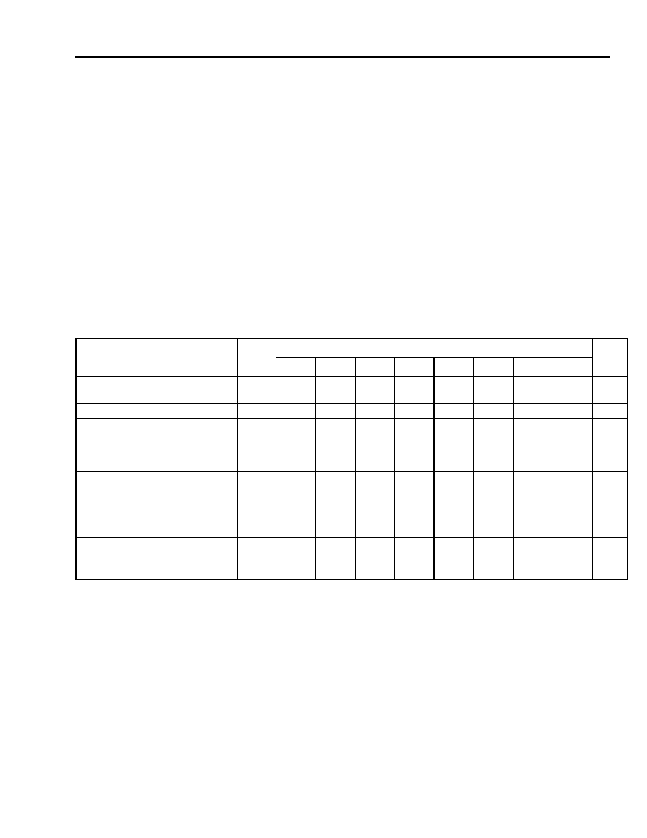
represented in Table 2.
Table 2
. ORCA Series 2 System Performance
1. Implemented using 4 x 1 multiplier mode (unpipelined), register-to-register, two 8-bit inputs, one 16-bit output.
2. Implemented using two 16 x 12 ROMs and one 12-bit adder, one 8-bit input, one fixed operand, one 16-bit output.
3. Implemented using 4 x 1 multiplier mode (fully pipelined), two 8-bit inputs, one 16-bit output (28 of 44 PFUs contain only pipelining registers).
4. Implemented using 16 x 4 synchronous single-port RAM mode allowing both read and write per clock cycle, including write/read address
multiplexer.
5. Implemented using 16 x 4 synchronous single-port RAM mode allowing either read or write per clock cycle, including write/read address mul-
tiplexer.
6. Implemented using 16 x 2 synchronous dual-port RAM mode.
7. OR2TxxB available only in -7 and -8 speeds only.
8. Speed grades of -5, -6, and -7 are for OR2TxxA devices only.
Function
#
PFUs
Speed Grade
Unit
-2A
-3A
-4A
-5A
-6A
-7A
-7B
-8B
16-bit loadable up/down
counter
4
51.0
66.7
87.0
104.2
129.9
144.9
131.6
149.3
MHz
16-bit accumulator
4
51.0
66.7
87.0
104.2
129.9
144.9
131.6
149.3
MHz
8 x 8 parallel multiplier:
— Multiplier mode, unpipelined1
— ROM mode, unpipelined2
— Multiplier mode, pipelined3
22
9
44
14.2
41.5
50.5
19.3
55.6
69.0
25.1
71.9
82.0
31.0
87.7
103.1
36.0
107.5
125.0
40.3
122.0
142.9
37.7
103.1
123.5
44.8
120.5
142.9
MHz
32 x 16 RAM:
— Single port (read and write/
cycle)4
— Single port5
— Dual port6
9
16
21.8
38.2
28.6
52.6
36.2
69.0
83.3
53.8
92.6
53.8
92.6
62.5
96.2
57.5
97.7
69.4
112.4
MHz
36-bit parity check (internal)
4
13.9
11.0
9.1
7.4
5.6
5.2
6.1
5.1
ns
32-bit address decode
(internal)
3.25
12.3
9.5
7.5
6.1
4.6
4.3
4.8
4.0
ns
相關(guān)PDF資料 |
PDF描述 |
|---|---|
| OR2T08A-5BA240I | Field-Programmable Gate Arrays |
| OR2T08A-5PS208I | Field-Programmable Gate Arrays |
| OR2T08A-5PS240 | Field-Programmable Gate Arrays |
| OR2T08A-5PS240I | Ceramic Chip Capacitors / MIL-PRF-55681; Capacitance [nom]: 2.2pF; Working Voltage (Vdc)[max]: 100V; Capacitance Tolerance: +/-0.1pF; Dielectric: Multilayer Ceramic; Temperature Coefficient: C0G (NP0); Lead Style: Surface Mount Chip; Lead Dimensions: 1206; Termination: Solder Coated SnPb; Body Dimensions: 0.125" x 0.062" x 0.051"; Container: Bag; Features: MIL-PRF-55681: P Failure Rate |
| OR2T08A-5PS256 | Field-Programmable Gate Arrays |
相關(guān)代理商/技術(shù)參數(shù) |
參數(shù)描述 |
|---|---|
| OR2T08A5BA256-DB | 功能描述:FPGA - 現(xiàn)場(chǎng)可編程門陣列 Use ECP/EC or XP RoHS:否 制造商:Altera Corporation 系列:Cyclone V E 柵極數(shù)量: 邏輯塊數(shù)量:943 內(nèi)嵌式塊RAM - EBR:1956 kbit 輸入/輸出端數(shù)量:128 最大工作頻率:800 MHz 工作電源電壓:1.1 V 最大工作溫度:+ 70 C 安裝風(fēng)格:SMD/SMT 封裝 / 箱體:FBGA-256 |
| OR2T08A5J160-DB | 功能描述:FPGA - 現(xiàn)場(chǎng)可編程門陣列 784 LUT 209 I/O RoHS:否 制造商:Altera Corporation 系列:Cyclone V E 柵極數(shù)量: 邏輯塊數(shù)量:943 內(nèi)嵌式塊RAM - EBR:1956 kbit 輸入/輸出端數(shù)量:128 最大工作頻率:800 MHz 工作電源電壓:1.1 V 最大工作溫度:+ 70 C 安裝風(fēng)格:SMD/SMT 封裝 / 箱體:FBGA-256 |
| OR2T08A5M84-D | 制造商:Lattice Semiconductor Corporation 功能描述: |
| OR2T08A5S208-DB | 功能描述:FPGA - 現(xiàn)場(chǎng)可編程門陣列 Use ECP/EC or XP RoHS:否 制造商:Altera Corporation 系列:Cyclone V E 柵極數(shù)量: 邏輯塊數(shù)量:943 內(nèi)嵌式塊RAM - EBR:1956 kbit 輸入/輸出端數(shù)量:128 最大工作頻率:800 MHz 工作電源電壓:1.1 V 最大工作溫度:+ 70 C 安裝風(fēng)格:SMD/SMT 封裝 / 箱體:FBGA-256 |
| OR2T08A5S240-DB | 功能描述:FPGA - 現(xiàn)場(chǎng)可編程門陣列 784 LUT 209 I/O RoHS:否 制造商:Altera Corporation 系列:Cyclone V E 柵極數(shù)量: 邏輯塊數(shù)量:943 內(nèi)嵌式塊RAM - EBR:1956 kbit 輸入/輸出端數(shù)量:128 最大工作頻率:800 MHz 工作電源電壓:1.1 V 最大工作溫度:+ 70 C 安裝風(fēng)格:SMD/SMT 封裝 / 箱體:FBGA-256 |
發(fā)布緊急采購(gòu),3分鐘左右您將得到回復(fù)。