- 您現(xiàn)在的位置:買賣IC網(wǎng) > PDF目錄224644 > OR2T06A-6T84I (Electronic Theatre Controls, Inc.) Field-Programmable Gate Arrays PDF資料下載
第1頁第2頁第3頁第4頁第5頁第6頁第7頁第8頁第9頁第10頁第11頁第12頁第13頁第14頁第15頁第16頁第17頁第18頁第19頁第20頁第21頁第22頁第23頁第24頁第25頁第26頁第27頁第28頁第29頁第30頁第31頁第32頁第33頁第34頁第35頁第36頁第37頁第38頁第39頁第40頁第41頁第42頁第43頁第44頁第45頁第46頁第47頁第48頁第49頁第50頁第51頁第52頁第53頁第54頁第55頁第56頁第57頁第58頁第59頁第60頁第61頁第62頁第63頁第64頁第65頁第66頁第67頁第68頁第69頁第70頁第71頁第72頁第73頁第74頁第75頁第76頁第77頁第78頁第79頁第80頁第81頁第82頁第83頁第84頁第85頁第86頁第87頁第88頁第89頁第90頁第91頁第92頁第93頁第94頁第95頁第96頁第97頁第98頁第99頁第100頁第101頁第102頁第103頁第104頁第105頁第106頁第107頁第108頁第109頁第110頁第111頁第112頁第113頁第114頁第115頁第116頁第117頁第118頁第119頁第120頁第121頁第122頁第123頁第124頁第125頁第126頁第127頁第128頁第129頁第130頁第131頁第132頁第133頁第134頁第135頁第136頁第137頁第138頁第139頁第140頁第141頁第142頁第143頁第144頁第145頁第146頁第147頁第148頁第149頁第150頁第151頁第152頁第153頁第154頁第155頁第156頁第157頁第158頁第159頁第160頁第161頁第162頁第163頁第164頁第165頁當前第166頁第167頁第168頁第169頁第170頁第171頁第172頁第173頁第174頁第175頁第176頁第177頁第178頁第179頁第180頁第181頁第182頁第183頁第184頁第185頁第186頁第187頁第188頁第189頁第190頁第191頁第192頁
Data Sheet
June 1999
ORCA Series 2 FPGAs
Lucent Technologies Inc.
75
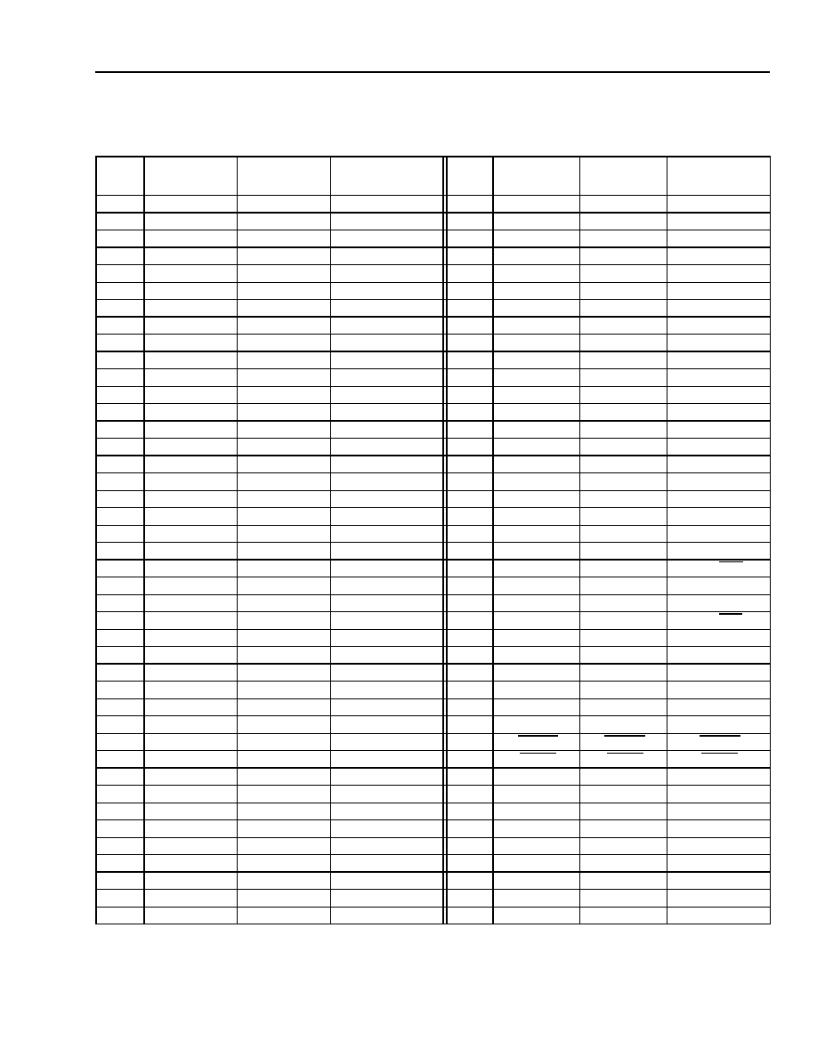
Pin Information (continued)
Table 21. OR2C/2T04A and OR2C/2T06A 144-Pin TQFP Pinout
Pin
2C/2T04A
Pad
2C/2T06A
Pad
Function
Pin
2C/2T04A
Pad
2C/2T06A
Pad
Function
1VDD
VDD
43
PB2B
PB3B
I/O
2VSS
VSS
44
PB2D
PB3D
I/O
3PL1C
PL1A
I/O-A0
45
VDD
4
PL1B
PL2D
I/O
46
PB3A
PB4A
I/O
5
PL1A
PL2A
I/O-A1
47
PB3D
PB4D
I/O
6
PL2D
PL3D
I/O-A2
48
PB4A
PB5A
I/O
7
PL2A
PL3A
I/O-A3
49
PB4C
PB5C
I/O
8
PL3D
PL4D
I/O
50
PB4D
PB5D
I/O
9
PL3C
PL4C
I/O
51
PB5A
PB6A
I/O
10
PL3A
PL4A
I/O-A4
52
PB5C
PB6C
I/O
11
PL4D
PL5D
I/O-A5
53
PB5D
PB6D
I/O
12
PL4C
PL5C
I/O
54
VSS
13
PL4A
PL5A
I/O-A6
55
PB6A
PB7A
I/O
14
VSS
56
PB6C
PB7C
I/O
15
PL5D
PL6D
I/O
57
PB6D
PB7D
I/O
16
PL5C
PL6C
I/O
58
PB7A
PB8A
I/O-VDD5
17
PL5A
PL6A
I/O-A7
59
PB7D
PB8D
I/O
18
VDD
60
PB8A
PB9A
I/O-HDC
19
PL6D
PL7D
I/O
61
PB8C
PB9C
I/O
20
PL6C
PL7C
I/O-VDD5
62
PB8D
PB9D
I/O
21
PL6A
PL7A
I/O-A8
63
VDD
22
VSS
64
PB9A
PB10A
I/O-LDC
23
PL7D
PL8D
I/O-A9
65
PB9C
PB10C
I/O
24
PL7A
PL8A
I/O-A10
66
PB9D
PB10D
I/O
25
PL8D
PL9D
I/O
67
PB10A
PB11A
I/O-INIT
26
PL8C
PL9C
I/O
68
PB10C
PB11D
I/O
27
PL8A
PL9A
I/O-A11
69
PB10D
PB12A
I/O
28
PL9D
PL10D
I/O-A12
70
VSS
29
PL9C
PL10C
I/O
71
DONE
30
PL9A
PL10A
I/O-A13
72
VDD
31
PL10D
PL11A
I/O-A14
73
VSS
32
PL10C
PL12D
I/O
74
RESET
33
PL10B
PL12B
I/O
75
PRGM
34
PL10A
PL12A
I/O-A15
76
PR10A
PR12A
I/O-M0
35
VSS
77
PR10B
PR12D
I/O
36
CCLK
78
PR10D
PR11A
I/O
37
VDD
79
PR9A
PR10A
I/O-M1
38
VSS
80
PR9C
PR10C
I/O
39
PB1A
I/O-A16
81
PR9D
PR10D
I/O
40
PB1C
PB1D
I/O
82
PR8A
PR9A
I/O-M2
41
PB1D
PB2A
I/O-A17
83
PR8B
PR9B
I/O
42
PB2A
PB3A
I/O
84
PR8D
PR9D
I/O
Note: The pins labeled I/O-VDD5 are user I/Os for the OR2CxxA and OR2TxxB series, but they are connected to VDD5 for the OR2TxxA
series.
相關PDF資料 |
PDF描述 |
|---|---|
| OR2T06A-7BA144 | Field-Programmable Gate Arrays |
| OR2T06A-7BA144I | Field-Programmable Gate Arrays |
| OR2T06A-7BA160 | Field-Programmable Gate Arrays |
| OR2T06A-7BA160I | Field-Programmable Gate Arrays |
| OR2T06A-7BA208 | Field-Programmable Gate Arrays |
相關代理商/技術參數(shù) |
參數(shù)描述 |
|---|---|
| OR2T06A-7BA100 | 制造商:未知廠家 制造商全稱:未知廠家 功能描述:Field-Programmable Gate Arrays |
| OR2T06A-7BA100I | 制造商:未知廠家 制造商全稱:未知廠家 功能描述:Field-Programmable Gate Arrays |
| OR2T06A-7BA144 | 制造商:未知廠家 制造商全稱:未知廠家 功能描述:Field-Programmable Gate Arrays |
| OR2T06A-7BA144I | 制造商:未知廠家 制造商全稱:未知廠家 功能描述:Field-Programmable Gate Arrays |
| OR2T06A-7BA160 | 制造商:未知廠家 制造商全稱:未知廠家 功能描述:Field-Programmable Gate Arrays |
發(fā)布緊急采購,3分鐘左右您將得到回復。