- 您現(xiàn)在的位置:買賣IC網(wǎng) > PDF目錄224641 > OR2C15A-5M352I (Electronic Theatre Controls, Inc.) Ceramic Chip Capacitors / MIL-PRF-55681; Capacitance [nom]: 430pF; Working Voltage (Vdc)[max]: 100V; Capacitance Tolerance: +/-1%; Dielectric: Multilayer Ceramic; Temperature Coefficient: C0G (NP0); Lead Style: Surface Mount Chip; Lead Dimensions: 0805; Termination: Base Metalization - Barrier Metal - 100% Tin; Body Dimensions: 0.080" x 0.050" x 0.055"; Container: Bag; Features: MIL-PRF-55681: S Failure Rate PDF資料下載
參數(shù)資料
| 型號(hào): | OR2C15A-5M352I |
| 廠商: | Electronic Theatre Controls, Inc. |
| 英文描述: | Ceramic Chip Capacitors / MIL-PRF-55681; Capacitance [nom]: 430pF; Working Voltage (Vdc)[max]: 100V; Capacitance Tolerance: +/-1%; Dielectric: Multilayer Ceramic; Temperature Coefficient: C0G (NP0); Lead Style: Surface Mount Chip; Lead Dimensions: 0805; Termination: Base Metalization - Barrier Metal - 100% Tin; Body Dimensions: 0.080" x 0.050" x 0.055"; Container: Bag; Features: MIL-PRF-55681: S Failure Rate |
| 中文描述: | 現(xiàn)場(chǎng)可編程門陣列 |
| 文件頁數(shù): | 190/192頁 |
| 文件大?。?/td> | 3148K |
| 代理商: | OR2C15A-5M352I |
第1頁第2頁第3頁第4頁第5頁第6頁第7頁第8頁第9頁第10頁第11頁第12頁第13頁第14頁第15頁第16頁第17頁第18頁第19頁第20頁第21頁第22頁第23頁第24頁第25頁第26頁第27頁第28頁第29頁第30頁第31頁第32頁第33頁第34頁第35頁第36頁第37頁第38頁第39頁第40頁第41頁第42頁第43頁第44頁第45頁第46頁第47頁第48頁第49頁第50頁第51頁第52頁第53頁第54頁第55頁第56頁第57頁第58頁第59頁第60頁第61頁第62頁第63頁第64頁第65頁第66頁第67頁第68頁第69頁第70頁第71頁第72頁第73頁第74頁第75頁第76頁第77頁第78頁第79頁第80頁第81頁第82頁第83頁第84頁第85頁第86頁第87頁第88頁第89頁第90頁第91頁第92頁第93頁第94頁第95頁第96頁第97頁第98頁第99頁第100頁第101頁第102頁第103頁第104頁第105頁第106頁第107頁第108頁第109頁第110頁第111頁第112頁第113頁第114頁第115頁第116頁第117頁第118頁第119頁第120頁第121頁第122頁第123頁第124頁第125頁第126頁第127頁第128頁第129頁第130頁第131頁第132頁第133頁第134頁第135頁第136頁第137頁第138頁第139頁第140頁第141頁第142頁第143頁第144頁第145頁第146頁第147頁第148頁第149頁第150頁第151頁第152頁第153頁第154頁第155頁第156頁第157頁第158頁第159頁第160頁第161頁第162頁第163頁第164頁第165頁第166頁第167頁第168頁第169頁第170頁第171頁第172頁第173頁第174頁第175頁第176頁第177頁第178頁第179頁第180頁第181頁第182頁第183頁第184頁第185頁第186頁第187頁第188頁第189頁當(dāng)前第190頁第191頁第192頁
Data Sheet
June 1999
ORCA Series 2 FPGAs
Lucent Technologies Inc.
97
B10
PT6D
PT7D
PT8D
PT9D
PT10D
I/O
C10
PT6C
PT7C
PT8C
PT9C
PT10C
I/O
D10
PT6B
PT7B
PT8B
PT9B
PT10B
I/O-VDD5
A9
PT6A
PT7A
PT8A
PT9A
PT10A
I/O-D2
B9
PT5D
PT6D
PT7D
PT8D
PT9D
I/O-D1
C9
PT5C
PT6C
PT7C
PT8C
PT9C
I/O
D9
PT5B
PT6B
PT7B
PT8B
PT9B
I/O
A8
PT5A
PT6A
PT7A
PT8A
PT9A
I/O-D0/DIN
B8
PT4D
PT5D
PT6D
PT7D
PT8D
I/O
C8
PT4C
PT5C
PT6C
PT7C
PT8C
I/O
A7
PT4B
PT5B
PT6B
PT7B
PT8B
I/O
B7
PT4A
PT5A
PT6A
PT7A
PT8A
I/O-DOUT
A6
PT3D
PT4D
PT5D
PT6D
PT7D
I/O
C7
PT3C
PT4C
PT5A
PT6A
PT7A
I/O
B6
PT3B
PT4B
PT4D
PT5C
PT6C
I/O
A5
PT3A
PT4A
PT5A
PT6A
I/O-TDI
D7
PT2D
PT3D
PT4D
PT5D
I/O
C6
PT2C
PT3C
PT4A
PT5A
I/O-VDD5
B5
PT2B
PT3B
PT3D
PT4D
I/O
A4
PT2A
PT3A
PT4A
I/O-TMS
C5
—
PT2D
PT3D
I/O
B4
PT1D
PT2C
PT3A
I/O
A3
PT1C
PT2B
PT2D
I/O
D5
PT1B
PT2A
I/O
C4
—
PT1D
I/O
B3
—
PT1C
I/O
B2
—
PT1B
I/O
A2
PT1A
I/O-TCK
C3
RD_DATA/TDO
A1
VSS
D4
VSS
D8
VSS
D13
VSS
D17
VSS
H4
VSS
H17
VSS
N4
VSS
N17
VSS
U4
VSS
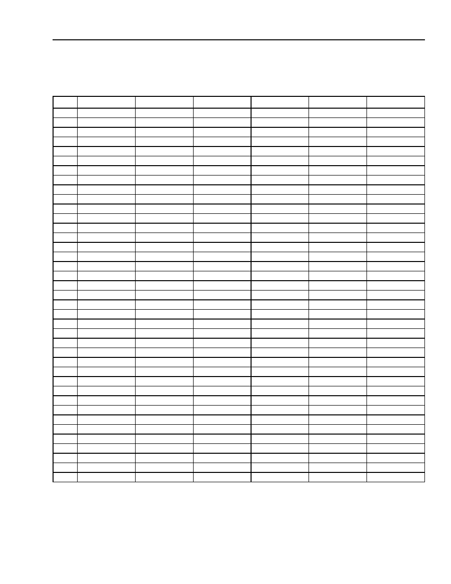
Pin Information (continued)
Table 25. OR2C/2T06A, OR2C/2T08A, OR2C/2T10A, OR2C/2T12A, and OR2C/2T15A/B
256-Pin PBGA Pinout (continued)
Pin
2C/2T06A Pad
2C/2T08A Pad
2C/2T10A Pad
2C/2T12A Pad
2C/2T15A/B Pad
Function
Notes:
The W3 pin on the 256-pin PBGA package is unconnected for all devices listed in this table.
The OR2C/2T08A do not have bond pads connected to the 256-pin PBGA package pins F2 and Y17.
The pins labeled I/O-VDD5 are user I/Os for the OR2CxxA and OR2TxxB series, but they are connected to VDD5 for the OR2TxxA series.
The pins labeled VSS-ETC are the 4 x 4 array of thermal balls located at the center of the package. The balls can be attached to the ground
plane of the board for enhanced thermal capability (see Table 29), or they can be left unconnected.
發(fā)布緊急采購,3分鐘左右您將得到回復(fù)。