- 您現(xiàn)在的位置:買賣IC網(wǎng) > PDF目錄224626 > OR2C06A-6PS208 (Electronic Theatre Controls, Inc.) Field-Programmable Gate Arrays PDF資料下載
參數(shù)資料
| 型號: | OR2C06A-6PS208 |
| 廠商: | Electronic Theatre Controls, Inc. |
| 元件分類: | FPGA |
| 英文描述: | Field-Programmable Gate Arrays |
| 中文描述: | 現(xiàn)場可編程門陣列 |
| 文件頁數(shù): | 46/192頁 |
| 文件大小: | 3148K |
| 代理商: | OR2C06A-6PS208 |
第1頁第2頁第3頁第4頁第5頁第6頁第7頁第8頁第9頁第10頁第11頁第12頁第13頁第14頁第15頁第16頁第17頁第18頁第19頁第20頁第21頁第22頁第23頁第24頁第25頁第26頁第27頁第28頁第29頁第30頁第31頁第32頁第33頁第34頁第35頁第36頁第37頁第38頁第39頁第40頁第41頁第42頁第43頁第44頁第45頁當(dāng)前第46頁第47頁第48頁第49頁第50頁第51頁第52頁第53頁第54頁第55頁第56頁第57頁第58頁第59頁第60頁第61頁第62頁第63頁第64頁第65頁第66頁第67頁第68頁第69頁第70頁第71頁第72頁第73頁第74頁第75頁第76頁第77頁第78頁第79頁第80頁第81頁第82頁第83頁第84頁第85頁第86頁第87頁第88頁第89頁第90頁第91頁第92頁第93頁第94頁第95頁第96頁第97頁第98頁第99頁第100頁第101頁第102頁第103頁第104頁第105頁第106頁第107頁第108頁第109頁第110頁第111頁第112頁第113頁第114頁第115頁第116頁第117頁第118頁第119頁第120頁第121頁第122頁第123頁第124頁第125頁第126頁第127頁第128頁第129頁第130頁第131頁第132頁第133頁第134頁第135頁第136頁第137頁第138頁第139頁第140頁第141頁第142頁第143頁第144頁第145頁第146頁第147頁第148頁第149頁第150頁第151頁第152頁第153頁第154頁第155頁第156頁第157頁第158頁第159頁第160頁第161頁第162頁第163頁第164頁第165頁第166頁第167頁第168頁第169頁第170頁第171頁第172頁第173頁第174頁第175頁第176頁第177頁第178頁第179頁第180頁第181頁第182頁第183頁第184頁第185頁第186頁第187頁第188頁第189頁第190頁第191頁第192頁
Data Sheet
ORCA Series 2 FPGAs
June 1999
14
Lucent Technologies Inc.
Programmable Logic Cells (continued)
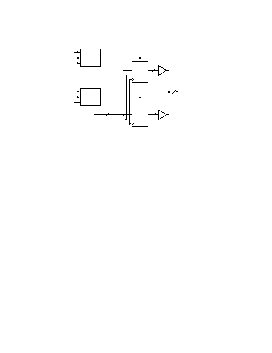
Note: The lower address bits are not shown.
Figure 16. Synchronous RAM with Write-Port Enable (WPE)
UPPER
ADDRESS
BITS
ADDRESS
DECODE
LUT1
BANK_EN1
UPPER
ADDRESS
BITS
ADDRESS
DECODE
LUT2
BANK_EN2
WR
DI
WPE
DO
16 x 4 RAM +
4 BUFFERS/PFU
BIDI
DOUT
4
WR
DI
WPE
DO
16 x 4 RAM +
4 BUFFERS/PFU
DIN
WR
CLK
4
BIDI
4
5-4640(F)
To increase memory word depth above 16 (e.g., 32 x
4), two or more PLCs can be used. The address and
write data inputs for the two or more PLCs are tied
together (bit by bit), and the data outputs are routed
through the four 3-statable BIDIs available in each
PFU. The BIDI outputs are then tied together (bit by
bit), as seen in Figure 16.
The control signals of the 3-statable BIDIs, called RAM
bank-enable (BANK_EN1 and BANK_EN2), are cre-
ated from a decode of upper address bits. The RAM
bank-enable is then used to enable 4 bits of data from
a PLC onto the read data (DOUT) bus.
The Series 2 series now has a new AND function avail-
able for each PFU in RAM mode. The inputs to this
function are the write-enable (WE) signal and the write-
port enable (WPE) signal. The write-enable signal is
input on A4, while the write-port enable is input on C0
or CIN. Generally, the WPE input is driven by the same
RAM bank-enable signal that controls the BIDIs in each
PFU.
The selection as to which RAM bank to write data into
does not require the use of LUTs from other PFUs, as
in previous
ORCA architectures. This reduces the num-
ber of PFUs required for RAMs larger than 16 words in
depth.
A special use of this method can be to increase word
depth to 32 words. Since both the WPE input into the
RAM and the 3-state input into the BIDI can be
inverted, a decode of the one upper address bit is not
required. Instead, the bank-enable signal for both
banks is tied to the upper address bit, with the WPE
and 3-state inputs active-high for one bank and active-
low for the other.
To increase the memory’s word size (e.g., 16 x 8), two
or more PLCs are used again. The address, write-
enable, and write-port enable of the PLCs are tied
together (bit by bit), and the data is different for each
PLC. Increasing both the address locations and word
size is accomplished by using a combination of these
two techniques.
相關(guān)PDF資料 |
PDF描述 |
|---|---|
| OR2C06A-6PS208I | Field-Programmable Gate Arrays |
| OR2C06A-6PS240 | Ceramic Chip Capacitors / MIL-PRF-55681; Capacitance [nom]: 0.033uF; Working Voltage (Vdc)[max]: 100V; Capacitance Tolerance: +/-10%; Dielectric: Multilayer Ceramic; Temperature Coefficient: X7R (BX); Lead Style: Surface Mount Chip; Lead Dimensions: 1808; Termination: Solder Coated SnPb; Body Dimensions: 0.180" x 0.080" x 0.080"; Container: Bag; Features: MIL-PRF-55681: M Failure Rate |
| OR2C06A-6PS240I | Field-Programmable Gate Arrays |
| OR2C06A-6PS256 | Field-Programmable Gate Arrays |
| OR2C06A-7BA144I | Field-Programmable Gate Arrays |
相關(guān)代理商/技術(shù)參數(shù) |
參數(shù)描述 |
|---|---|
| OR2C06A-6PS208I | 制造商:未知廠家 制造商全稱:未知廠家 功能描述:Field-Programmable Gate Arrays |
| OR2C06A-6PS240 | 制造商:未知廠家 制造商全稱:未知廠家 功能描述:Field-Programmable Gate Arrays |
| OR2C06A-6PS240I | 制造商:未知廠家 制造商全稱:未知廠家 功能描述:Field-Programmable Gate Arrays |
| OR2C06A-6PS256 | 制造商:未知廠家 制造商全稱:未知廠家 功能描述:Field-Programmable Gate Arrays |
| OR2C06A-6PS256I | 制造商:未知廠家 制造商全稱:未知廠家 功能描述:Field-Programmable Gate Arrays |
發(fā)布緊急采購,3分鐘左右您將得到回復(fù)。