- 您現(xiàn)在的位置:買賣IC網(wǎng) > PDF目錄224626 > OR2C06A-6M84I (Electronic Theatre Controls, Inc.) Field-Programmable Gate Arrays PDF資料下載
參數(shù)資料
| 型號(hào): | OR2C06A-6M84I |
| 廠商: | Electronic Theatre Controls, Inc. |
| 元件分類: | FPGA |
| 英文描述: | Field-Programmable Gate Arrays |
| 中文描述: | 現(xiàn)場(chǎng)可編程門(mén)陣列 |
| 文件頁(yè)數(shù): | 151/192頁(yè) |
| 文件大?。?/td> | 3148K |
| 代理商: | OR2C06A-6M84I |
第1頁(yè)第2頁(yè)第3頁(yè)第4頁(yè)第5頁(yè)第6頁(yè)第7頁(yè)第8頁(yè)第9頁(yè)第10頁(yè)第11頁(yè)第12頁(yè)第13頁(yè)第14頁(yè)第15頁(yè)第16頁(yè)第17頁(yè)第18頁(yè)第19頁(yè)第20頁(yè)第21頁(yè)第22頁(yè)第23頁(yè)第24頁(yè)第25頁(yè)第26頁(yè)第27頁(yè)第28頁(yè)第29頁(yè)第30頁(yè)第31頁(yè)第32頁(yè)第33頁(yè)第34頁(yè)第35頁(yè)第36頁(yè)第37頁(yè)第38頁(yè)第39頁(yè)第40頁(yè)第41頁(yè)第42頁(yè)第43頁(yè)第44頁(yè)第45頁(yè)第46頁(yè)第47頁(yè)第48頁(yè)第49頁(yè)第50頁(yè)第51頁(yè)第52頁(yè)第53頁(yè)第54頁(yè)第55頁(yè)第56頁(yè)第57頁(yè)第58頁(yè)第59頁(yè)第60頁(yè)第61頁(yè)第62頁(yè)第63頁(yè)第64頁(yè)第65頁(yè)第66頁(yè)第67頁(yè)第68頁(yè)第69頁(yè)第70頁(yè)第71頁(yè)第72頁(yè)第73頁(yè)第74頁(yè)第75頁(yè)第76頁(yè)第77頁(yè)第78頁(yè)第79頁(yè)第80頁(yè)第81頁(yè)第82頁(yè)第83頁(yè)第84頁(yè)第85頁(yè)第86頁(yè)第87頁(yè)第88頁(yè)第89頁(yè)第90頁(yè)第91頁(yè)第92頁(yè)第93頁(yè)第94頁(yè)第95頁(yè)第96頁(yè)第97頁(yè)第98頁(yè)第99頁(yè)第100頁(yè)第101頁(yè)第102頁(yè)第103頁(yè)第104頁(yè)第105頁(yè)第106頁(yè)第107頁(yè)第108頁(yè)第109頁(yè)第110頁(yè)第111頁(yè)第112頁(yè)第113頁(yè)第114頁(yè)第115頁(yè)第116頁(yè)第117頁(yè)第118頁(yè)第119頁(yè)第120頁(yè)第121頁(yè)第122頁(yè)第123頁(yè)第124頁(yè)第125頁(yè)第126頁(yè)第127頁(yè)第128頁(yè)第129頁(yè)第130頁(yè)第131頁(yè)第132頁(yè)第133頁(yè)第134頁(yè)第135頁(yè)第136頁(yè)第137頁(yè)第138頁(yè)第139頁(yè)第140頁(yè)第141頁(yè)第142頁(yè)第143頁(yè)第144頁(yè)第145頁(yè)第146頁(yè)第147頁(yè)第148頁(yè)第149頁(yè)第150頁(yè)當(dāng)前第151頁(yè)第152頁(yè)第153頁(yè)第154頁(yè)第155頁(yè)第156頁(yè)第157頁(yè)第158頁(yè)第159頁(yè)第160頁(yè)第161頁(yè)第162頁(yè)第163頁(yè)第164頁(yè)第165頁(yè)第166頁(yè)第167頁(yè)第168頁(yè)第169頁(yè)第170頁(yè)第171頁(yè)第172頁(yè)第173頁(yè)第174頁(yè)第175頁(yè)第176頁(yè)第177頁(yè)第178頁(yè)第179頁(yè)第180頁(yè)第181頁(yè)第182頁(yè)第183頁(yè)第184頁(yè)第185頁(yè)第186頁(yè)第187頁(yè)第188頁(yè)第189頁(yè)第190頁(yè)第191頁(yè)第192頁(yè)
Lucent Technologies Inc.
61
Data Sheet
June 1999
ORCA Series 2 FPGAs
ORCA Timing Characteristics
(continued)
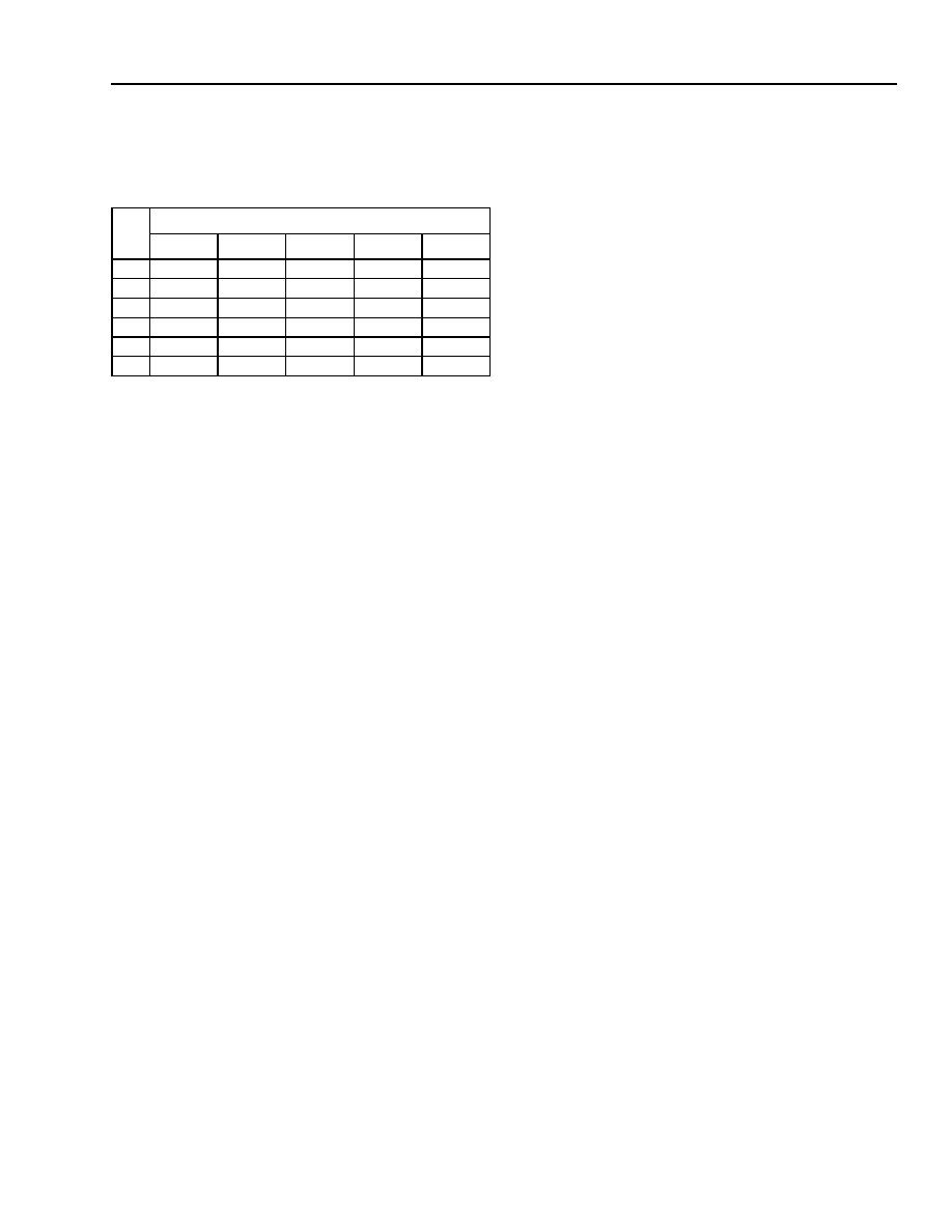
Table 15B. Derating for Commercial/Industrial
Devices (OR2TxxB)
Note: The derating tables shown above are for a typical critical path
that contains 33% logic delay and 66% routing delay. Since the
routing delay derates at a higher rate than the logic delay, paths
with more than 66% routing delay will derate at a higher rate
than shown in the table. The approximate derating values vs.
temperature are 0.26% per °C for logic delay and 0.45% per °C
for routing delay. The approximate derating values vs. voltage
are 0.13% per mV for both logic and routing delays at 25 °C.
In addition to supply voltage, process variation, and
operating temperature, circuit and process improve-
ments of the
ORCA series FPGAs over time will result
in significant improvement of the actual performance
over those listed for a speed grade. Even though lower
speed grades may still be available, the distribution of
yield to timing parameters may be several speed bins
higher than that designated on a product brand. Design
practices need to consider best-case timing parame-
ters (e.g., delays = 0), as well as worst-case timing.
The routing delays are a function of fan-out and the
capacitance associated with the CIPs and metal inter-
connect in the path. The number of logic elements that
can be driven (or fan-out) by PFUs is unlimited,
although the delay to reach a valid logic level can
exceed timing requirements. It is difficult to make accu-
rate routing delay estimates prior to design compilation
based on fan-out. This is because the CAE software
may delete redundant logic inserted by the designer to
reduce fan-out, and/or it may also automatically reduce
fan-out by net splitting.
The waveform test points are given in the Measure-
ment Conditions section of this data sheet. The timing
parameters given in the electrical characteristics tables
in this data sheet follow industry practices, and the val-
ues they reflect are described below.
s
Propagation Delay—the time between the specified
reference points. The delays provided are the worst
case of the tphh and tpll delays for noninverting func-
tions, tplh and tphl for inverting functions, and tphz
and tplz for 3-state enable.
s
Setup Time—the interval immediately preceding the
transition of a clock or latch enable signal, during
which the data must be stable to ensure it is recog-
nized as the intended value.
s
Hold Time—the interval immediately following the
transition of a clock or latch enable signal, during
which the data must be held stable to ensure it is rec-
ognized as the intended value.
s
3-state Enable—the time from when a TS[3:0] signal
becomes active and the output pad reaches the high-
impedance state.
Estimating Power Dissipation
OR2CxxA
The total operating power dissipated is estimated by
summing the standby (IDDSB), internal, and external
power dissipated. The internal and external power is
the power consumed in the PLCs and PICs, respec-
tively. In general, the standby power is small and may
be neglected. The total operating power is as follows:
PT =
Σ PPLC + Σ PPIC
The internal operating power is made up of two parts:
clock generation and PFU output power. The PFU out-
put power can be estimated based upon the number of
PFU outputs switching when driving an average fan-out
of two:
PPFU = 0.16 mW/MHz
For each PFU output that switches, 0.16 mW/MHz
needs to be multiplied times the frequency (in MHz)
that the output switches. Generally, this can be esti-
mated by using one-half the clock rate, multiplied by
some activity factor; for example, 20%.
The power dissipated by the clock generation circuitry
is based upon four parts: the fixed clock power, the
power/clock branch row or column, the clock power dis-
sipated in each PFU that uses this particular clock, and
the power from the subset of those PFUs that is config-
ured in either of the two synchronous modes (SSPM or
SDPM). Therefore, the clock power can be calculated
for the four parts using the following equations:
OR2C04A Clock Power
P
= [0.62 mW/MHz
+ (0.22 mW/MHz – Branch) (# Branches)
+ (0.022 mW/MHz – PFU) (# PFUs)
+ (0.006 mW/MHz – SMEM_PFU)
(# SMEM_PFUs)] fCLK
For a quick estimate, the worst-case (typical circuit)
OR2C04A clock power
≈ 3.9 mW/MHz.
TJ
(°C)
Power Supply Voltage
3.0 V
3.15 V
3.3 V
3.45 V
3.6 V
–40
0.81
0.78
0.76
0.74
0.73
0
0.86
0.83
0.80
0.77
0.76
25
0.9
0.87
0.83
0.8
0.78
85
1.0
0.95
0.93
0.88
0.86
100
1.02
0.98
0.95
0.91
0.88
125
1.06
1.03
0.98
0.95
0.92
相關(guān)PDF資料 |
PDF描述 |
|---|---|
| OR2C06A-6PS208 | Field-Programmable Gate Arrays |
| OR2C06A-6PS208I | Field-Programmable Gate Arrays |
| OR2C06A-6PS240 | Ceramic Chip Capacitors / MIL-PRF-55681; Capacitance [nom]: 0.033uF; Working Voltage (Vdc)[max]: 100V; Capacitance Tolerance: +/-10%; Dielectric: Multilayer Ceramic; Temperature Coefficient: X7R (BX); Lead Style: Surface Mount Chip; Lead Dimensions: 1808; Termination: Solder Coated SnPb; Body Dimensions: 0.180" x 0.080" x 0.080"; Container: Bag; Features: MIL-PRF-55681: M Failure Rate |
| OR2C06A-6PS240I | Field-Programmable Gate Arrays |
| OR2C06A-6PS256 | Field-Programmable Gate Arrays |
相關(guān)代理商/技術(shù)參數(shù) |
參數(shù)描述 |
|---|---|
| OR2C06A-6PS100 | 制造商:未知廠家 制造商全稱:未知廠家 功能描述:Field-Programmable Gate Arrays |
| OR2C06A-6PS100I | 制造商:未知廠家 制造商全稱:未知廠家 功能描述:Field-Programmable Gate Arrays |
| OR2C06A-6PS144 | 制造商:未知廠家 制造商全稱:未知廠家 功能描述:Field-Programmable Gate Arrays |
| OR2C06A-6PS144I | 制造商:未知廠家 制造商全稱:未知廠家 功能描述:Field-Programmable Gate Arrays |
| OR2C06A-6PS160 | 制造商:未知廠家 制造商全稱:未知廠家 功能描述:Field-Programmable Gate Arrays |
發(fā)布緊急采購(gòu),3分鐘左右您將得到回復(fù)。