- 您現(xiàn)在的位置:買(mǎi)賣(mài)IC網(wǎng) > PDF目錄376245 > OP497 (Analog Devices, Inc.) Precision Picoampere Input Current Quad Operational Amplifier PDF資料下載
參數(shù)資料
| 型號(hào): | OP497 |
| 廠商: | Analog Devices, Inc. |
| 英文描述: | Precision Picoampere Input Current Quad Operational Amplifier |
| 中文描述: | 精密Picoampere輸入電流四路運(yùn)算放大器 |
| 文件頁(yè)數(shù): | 3/12頁(yè) |
| 文件大小: | 302K |
| 代理商: | OP497 |
REV. D
OP497
–3–
ORDERING GUIDE
Temperature
Range
–55
°
C to +125
°
C
Package
Description
Package
Option
Model
OP497AY
*
OP497CY
*
–55
°
C to +125
°
C
OP497FP
–40
°
C to +85
°
C
OP497FS
–40
°
C to +85
°
C
OP497GP
–40
°
C to +85
°
C
OP497GS
–40
°
C to +85
°
C
*
Not for new design; obsolete April 2002.
14-Lead Cerdip
14-Lead Cerdip
14-Lead Plastic DIP N-14
16-Lead SOIC
14-Lead Plastic DIP N-14
16-Lead SOIC
Q-14
Q-14
R-16
R-16
For a military processed devices, please refer to the Standard
Microcircuit Drawing (SMD) available at www.dscc.dla.mil/
programs.milspec./default.asp.
SMD Part Number
ADI Part Number
5962–9452101M2A
*
5962–9452101MCA
OP497BRC
OP497BY
*
Not for new designs; obsolete April 2002.
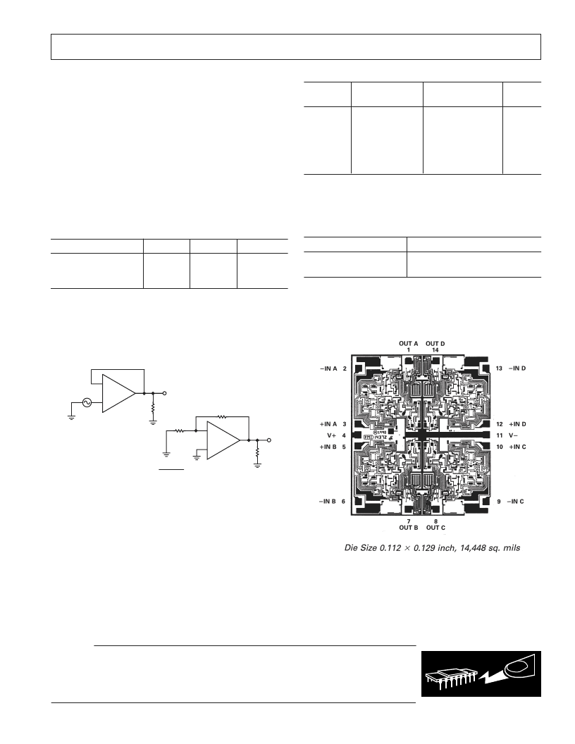
DICE CHARACTERISTICS
ABSOLUTE MAXIMUM RATINGS
1
Supply Voltage . . . . . . . . . . . . . . . . . . . . . . . . . . . . . . . .
±
20 V
Input Voltage
2 . . . . . . . . . . . . . . . . . . . . . . . . . . . . . . . . . . . . . . . . . . . . . . . . .
20 V
Differential Input Voltage
2
Output Short-Circuit Duration . . . . . . . . . . . . . . . . Indefinite
Storage Temperature Range
Y Package . . . . . . . . . . . . . . . . . . . . . . . . –65
°
C to +175
°
C
P, S Package . . . . . . . . . . . . . . . . . . . . . . . –65
°
C to +150
°
C
Operating Temperature Range
OP497A, C (Y) . . . . . . . . . . . . . . . . . . . . –55
°
C to +125
°
C
OP497F, G (Y) . . . . . . . . . . . . . . . . . . . . . –40
°
C to +85
°
C
OP497F, G (P, S) . . . . . . . . . . . . . . . . . . . –40
°
C to +85
°
C
Junction Temperature
Y Package . . . . . . . . . . . . . . . . . . . . . . . . –65
°
C to +175
°
C
P, S Package . . . . . . . . . . . . . . . . . . . . . . . –65
°
C to +150
°
C
Lead Temperature Range (Soldering 60 sec) . . . . . . . . 300
°
C
. . . . . . . . . . . . . . . . . . . . . . . . . . . . . . . . . .
40 V
Package Type
JA3
94
76
92
JC
Unit
°
C/W
°
C/W
°
C/W
14-Pin Cerdip (Y)
14-Pin Plastic DIP (P)
16-Pin SOIC (S)
NOTES
1
Absolute Maximum Ratings apply to both DICE and packaged parts, unless
otherwise noted.
2
For supply voltages less than
±
20 V, the absolute maximum input voltage is
equal to the supply voltage.
3
HIA is specified for worst-case mounting conditions, i.e.,
device in socket for cerdip, P-DIP packages;
to printed circuit board for SOIC package.
10
33
23
is specified for
JA
is specified for device soldered
1/4
OP497
+
V
2
2k
V
1
20V p
–
p @ 10Hz
CHANNEL SEPARATION = 20 log
V /10000
2
V
1
(
)
–
50
50k
–
+
OP497
Channel Separation Test Circuit
CAUTION
ESD (electrostatic discharge) sensitive device. Electrostatic charges as high as 4000 V readily
accumulate on the human body and test equipment and can discharge without detection. Although
the OP497 features proprietary ESD protection circuitry, permanent damage may occur on devices
subjected to high-energy electrostatic discharges. Therefore, proper ESD precautions are
recommended to avoid performance degradation or loss of functionality.
WARNING!
ESD SENSITIVE DEVICE
相關(guān)PDF資料 |
PDF描述 |
|---|---|
| OP497AY | Precision Picoampere Input Current Quad Operational Amplifier |
| OP497CY | Precision Picoampere Input Current Quad Operational Amplifier |
| OP497FP | Precision Picoampere Input Current Quad Operational Amplifier |
| OP497FS | Precision Picoampere Input Current Quad Operational Amplifier |
| OP497GP | Precision Picoampere Input Current Quad Operational Amplifier |
相關(guān)代理商/技術(shù)參數(shù) |
參數(shù)描述 |
|---|---|
| OP-497 | 制造商:AD 制造商全稱(chēng):Analog Devices 功能描述:PRECISION PICOAMPERE INPUT CURRENT QUAD OPERATIONAL AMPLIFIER |
| OP4970027SR | 制造商:Analog Devices 功能描述: |
| OP497AY | 制造商:AD 制造商全稱(chēng):Analog Devices 功能描述:Precision Picoampere Input Current Quad Operational Amplifier |
| OP-497AY | 制造商:AD 制造商全稱(chēng):Analog Devices 功能描述:PRECISION PICOAMPERE INPUT CURRENT QUAD OPERATIONAL AMPLIFIER |
| OP-497BRC/883 | 制造商:AD 制造商全稱(chēng):Analog Devices 功能描述:PRECISION PICOAMPERE INPUT CURRENT QUAD OPERATIONAL AMPLIFIER |
發(fā)布緊急采購(gòu),3分鐘左右您將得到回復(fù)。