- 您現(xiàn)在的位置:買賣IC網(wǎng) > PDF目錄224618 > NX2117ACUTR (MICROSEMI CORP-ANALOG MIXED SIGNAL GROUP) SWITCHING CONTROLLER, PDSO10 PDF資料下載
參數(shù)資料
| 型號: | NX2117ACUTR |
| 廠商: | MICROSEMI CORP-ANALOG MIXED SIGNAL GROUP |
| 元件分類: | 穩(wěn)壓器 |
| 英文描述: | SWITCHING CONTROLLER, PDSO10 |
| 封裝: | LEAD FREE, PLASTIC, MSOP-10 |
| 文件頁數(shù): | 4/14頁 |
| 文件大小: | 405K |
| 代理商: | NX2117ACUTR |
NX2116/2116A/2116B/2117/2117A
12
Rev. 3.0
03/14/06
4.Calculate R
3 value by the following equation.
OSC
O
OUT
3
in
ESR
m
REF
V
2
F
LV
1
R=
V
R
gV
1.5V
2
60kHz 1uH1
=
12V
6.5m
2.0mA/V
1.8V
0.8V
=8.15k
×π ××
×
××
×π ××
××
×
Choose R
3 =8.2k.
5. Calculate C
1 by setting compensator zero FZ
at 75% of the LC double pole.
1
3z
1
C =
2
RF
1
=
2
8.2k
0.75 2.9kHz
=8.9nF
×π ××
×π ×
××
Choose C
1=8.2nF.
6. Calculate C
2 by setting compensator pole
p
F
at half the swithing frequency.
2
3s
1
C =
RF
1
=
8 .2 k
300k Hz
=129pF
π ××
π ×
×
Choose C
1=120pF.
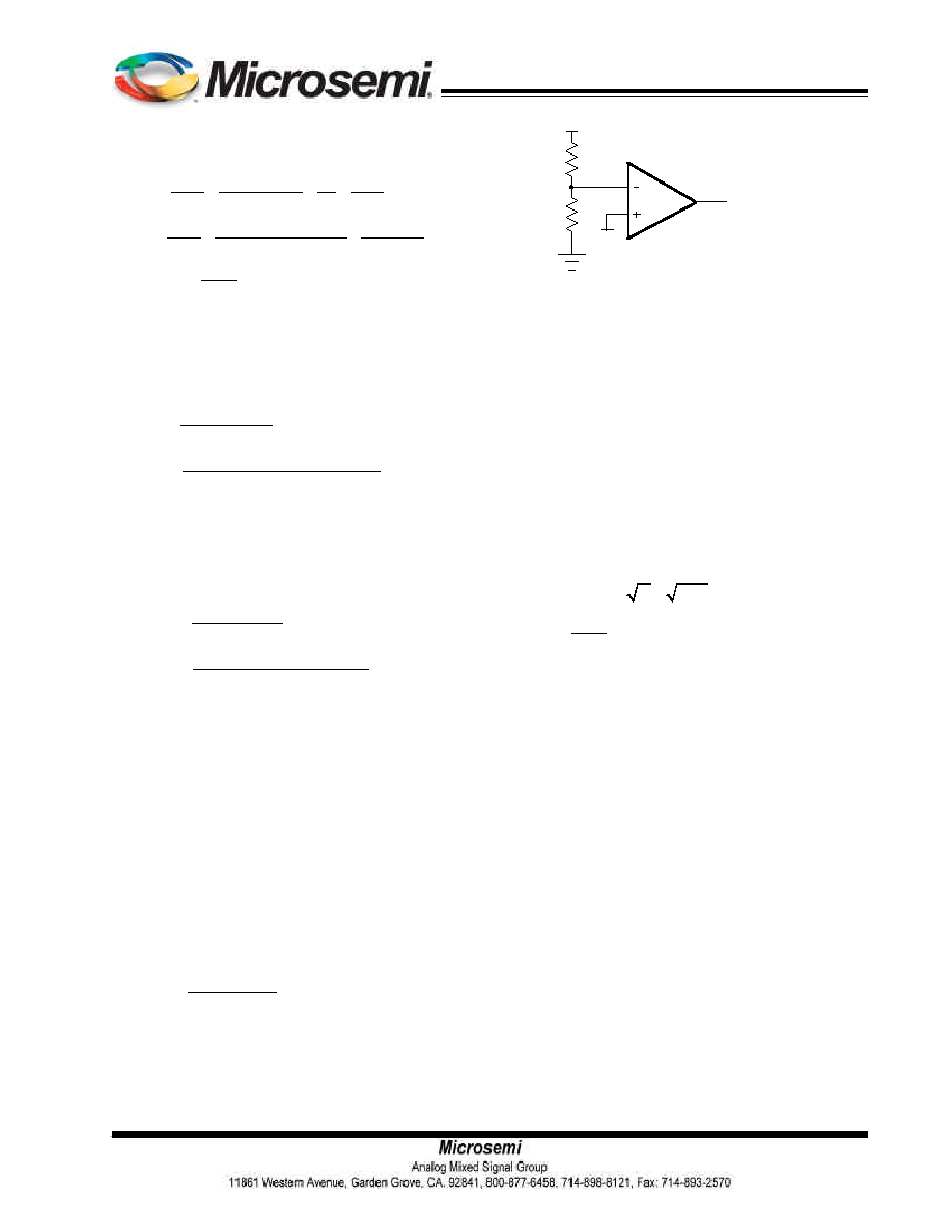
Output Voltage Calculation
Output voltage is set by reference voltage and ex-
ternal voltage divider. The reference voltage is fixed at
0.8V. The divider consists of two ratioed resistors so
that the output voltage applied at the Fb pin is 0.8V when
the output voltage is at the desired value. The following
equation and picture show the relationship between
OUT
V
,
REF
V
and voltage divider..
2
REF
1
OUT
REF
RV
R=
V
-V
×
...(18)
where R2 is part of the compensator, and the value
of R1 value can be set by voltage divider.
See compensator design for R
1 and R2 selection.
Vout
Vref
Fb
R2
R1
Voltage divider
Figure 8 - Voltage divider
Input Capacitor Selection
Input capacitors are usually a mix of high frequency
ceramic capacitors and bulk capacitors. Ceramic ca-
pacitors bypass the high frequency noise, and bulk ca-
pacitors supply switching current to the MOSFETs. Usu-
ally 1uF ceramic capacitor is chosen to decouple the
high frequency noise.The bulk input capacitors are de-
cided by voltage rating and RMS current rating. The RMS
current in the input capacitors can be calculated as:
RMS
OUT
IN
I
D
1-D
V
D
V
=
××
=
...(19)
VIN = 12V, VOUT=1.8V, IOUT=9A, using equation (19),
the result of input RMS current is 3.2A.
For higher efficiency, low ESR capacitors are rec-
ommended. One Sanyo OS-CON 16SP180M 16V 180uF
20m
with 3.4A RMS rating is chosen as input bulk
capacitors.
Power MOSFETs Selection
The power stage requires two N-Channel power
MOSFETs. The selection of MOSFETs is based on
maximum drain source voltage, gate source voltage,
maximum current rating, MOSFET on resistance and
power dissipation. The main consideration is the power
loss contribution of MOSFETs to the overall converter
efficiency. In this design example, two IRFR3709Z are
used. They have the following parameters: V
DS=30V,RDSON
=6.5m
,Q
GATE =17nC.
There are two factors causing the MOSFET power
loss:conduction loss, switching loss.
Conduction loss is simply defined as:
相關(guān)PDF資料 |
PDF描述 |
|---|---|
| NX25P16-VSI | 16M X 1 FLASH 2.7V PROM, PDSO8 |
| NX3225SA-100.000M-STD-CSR-3 | QUARTZ CRYSTAL RESONATOR, 100 MHz |
| NX5A0AE01 | MALE, STRAIGHT TWO PART BOARD CONNECTOR, PRESS FIT |
| NX5B0AE01 | MALE, STRAIGHT TWO PART BOARD CONNECTOR, PRESS FIT |
| NX5C0AE01 | MALE, STRAIGHT TWO PART BOARD CONNECTOR, PRESS FIT |
相關(guān)代理商/技術(shù)參數(shù) |
參數(shù)描述 |
|---|---|
| NX2117CUTR | 制造商:MICROSEMI 制造商全稱:Microsemi Corporation 功能描述:SYNCHRONOUS PWM CONTROLLER WITH CURRENT LIMIT, POWER GOOD & OVER VOLTAGE |
| NX2119 | 制造商:MICROSEMI 制造商全稱:Microsemi Corporation 功能描述:SYNCHRONOUS PWM CONTROLLER WITH CURRENT LIMIT PROTECTION |
| NX2119A | 制造商:MICROSEMI 制造商全稱:Microsemi Corporation 功能描述:SYNCHRONOUS PWM CONTROLLER WITH CURRENT LIMIT PROTECTION |
| NX2119ACSTR | 制造商:MICROSEMI 制造商全稱:Microsemi Corporation 功能描述:SYNCHRONOUS PWM CONTROLLER WITH CURRENT LIMIT PROTECTION |
| NX2119ACUTR | 制造商:MICROSEMI 制造商全稱:Microsemi Corporation 功能描述:SYNCHRONOUS PWM CONTROLLER WITH CURRENT LIMIT PROTECTION |
發(fā)布緊急采購,3分鐘左右您將得到回復(fù)。