- 您現(xiàn)在的位置:買賣IC網(wǎng) > PDF目錄363350 > NM24W17UTLZEN (FAIRCHILD SEMICONDUCTOR CORP) 16K-Bit Serial EEPROM 2-Wire Bus Interface PDF資料下載
參數(shù)資料
| 型號: | NM24W17UTLZEN |
| 廠商: | FAIRCHILD SEMICONDUCTOR CORP |
| 元件分類: | PROM |
| 英文描述: | 16K-Bit Serial EEPROM 2-Wire Bus Interface |
| 中文描述: | 2K X 8 I2C/2-WIRE SERIAL EEPROM, PDIP8 |
| 封裝: | PLASTIC, DIP-8 |
| 文件頁數(shù): | 8/13頁 |
| 文件大?。?/td> | 109K |
| 代理商: | NM24W17UTLZEN |
8
www.fairchildsemi.com
NM24C16U/17U Rev. B.1
N
DS800010-10
SDA
SCL
STOP
CONDITION
START
CONDITION
WORD n
8th BIT
ACK
tWR
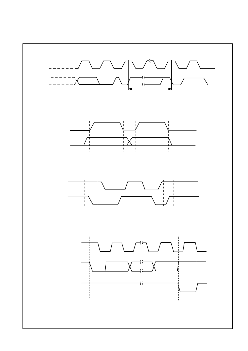
Write Cycle Timing (Figure 1)
Note:
The write cycle time (t
WR
) is the time from a valid stop condition of a write sequence to the end of the internal erase/program cycle.
Data Validity (Figure 2)
Start and Stop Definition (Figure 3)
Acknowledge Response from Receiver (Figure 4)
SCL FROM
MASTER
DATA OUTPUT
FROM
TRANSMITTER
DATA OUTPUT
FROM
RECEIVER
1
8
9
START
ACKNOWLEDGE
SDA
SCL
START
CONDITION
STOP
CONDITION
SCL
DATA STABLE
DATA
CHANGE
SDA
DS800010-11
DS800010-12
DS800010-13
相關(guān)PDF資料 |
PDF描述 |
|---|---|
| NM24W17UTLZM8 | 16K-Bit Serial EEPROM 2-Wire Bus Interface |
| NM24W17UTLZMT8 | 16K-Bit Serial EEPROM 2-Wire Bus Interface |
| NM24W17UTLZN | 16K-Bit Serial EEPROM 2-Wire Bus Interface |
| NM24W17UTLZVM8 | 16K-Bit Serial EEPROM 2-Wire Bus Interface |
| NM24W17UTLZVMT8 | 16K-Bit Serial EEPROM 2-Wire Bus Interface |
相關(guān)代理商/技術(shù)參數(shù) |
參數(shù)描述 |
|---|---|
| NM-250 | 制造商:WALDOM ELECTRONICS 功能描述: |
| NM-250-0015P | 制造商:WALDOM ELECTRONICS 功能描述: |
| NM-250-0025P | 制造商:WALDOM ELECTRONICS 功能描述: |
| NM25001S00 | 制造商:RadiSys 功能描述:LVDS;ADDCARD;BG845&LS855 |
| NM25C020 | 制造商:FAIRCHILD 制造商全稱:Fairchild Semiconductor 功能描述:2K-Bit Serial CMOS EEPROM (Serial Peripheral Interface (SPI) Synchronous Bus) |
發(fā)布緊急采購,3分鐘左右您將得到回復(fù)。