- 您現(xiàn)在的位置:買賣IC網(wǎng) > PDF目錄361122 > NLAST44599 (ON SEMICONDUCTOR) Low Voltage Single Supply Dual DPDT Analog Switch PDF資料下載
參數(shù)資料
| 型號(hào): | NLAST44599 |
| 廠商: | ON SEMICONDUCTOR |
| 英文描述: | Low Voltage Single Supply Dual DPDT Analog Switch |
| 中文描述: | 低電壓單電源雙DPDT模擬開關(guān) |
| 文件頁數(shù): | 5/12頁 |
| 文件大?。?/td> | 90K |
| 代理商: | NLAST44599 |
NLAST44599
http://onsemi.com
5
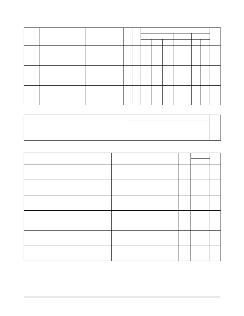
AC ELECTRICAL CHARACTERISTICS
(Input t
r
= t
f
= 3.0 ns)
Guaranteed Maximum Limit
V
CC
V
IS
55 C to 25 C
85 C
125 C
Symbol
Parameter
Test Conditions
(V)
(V)
Min
Typ*
Max
Min
Max
Min
Max
Unit
t
ON
Turn–On Time
(Figures 12 and 13)
R
L
= 300
(Figures 5 and 6)
C
L
= 35 pF
2.5
3.0
4.5
5.5
2.0
2.0
3.0
3.0
5
5
2
2
23
16
11
9
35
24
16
14
5
5
2
2
38
27
19
17
5
5
2
2
41
30
22
20
ns
t
OFF
Turn–Off Time
(Figures 12 and 13)
R
L
= 300
(Figures 5 and 6)
C
L
= 35 pF
2.5
3.0
4.5
5.5
2.0
2.0
3.0
3.0
1
1
1
1
7
5
4
3
12
10
6
5
1
1
1
1
15
13
9
8
1
1
1
1
18
16
12
11
ns
t
BBM
Minimum Break–Before–Make
Time
V
IS
= 3.0 V (Figure 4)
R
L
= 300
C
L
= 35 pF
2.5
3.0
4.5
5.5
2.0
2.0
3.0
1
1
1
1
12
11
6
5
1
1
1
1
1
1
1
1
ns
*Typical Characteristics are at 25 C.
Typical @ 25, VCC = 5.0 V
C
IN
C
NO
or
C
NC
C
COM
C
(ON)
Maximum Input Capacitance, Select Input
Analog I/O (Switch Off)
Common I/O (Switch Off)
Feedthrough (Switch On)
8
10
10
20
pF
ADDITIONAL APPLICATION CHARACTERISTICS
(Voltages Referenced to GND Unless Noted)
V
CC
V
Typical
Symbol
Parameter
Condition
25 C
Unit
BW
Maximum On–Channel
Minimum Frequency Response
(Figure 11)
3 dB Bandwidth or
V
IN
=
0 dBm
V
IN
centered between V
CC
and GND
(Figure 7)
3.0
4.5
5.5
145
170
175
MHz
V
ONL
Maximum Feedthrough On Loss
V
IN
=
0 dBm @ 100 kHz to 50 MHz
V
IN
centered between V
CC
and GND
(Figure 7)
3.0
4.5
5.5
–3
–3
–3
dB
V
ISO
Off–Channel Isolation
(Figure 10)
f = 100 kHz; V
IS
=
1 V RMS
V
IN
centered between V
CC
and GND
(Figure 7)
3.0
4.5
5.5
–93
–93
–93
dB
Q
Charge Injection Select Input to Common I/O
(Figure 15)
V
IN =
V
CC
to GND, F
IS
= 20 kHz
t
r
= t
f
= 3 ns
R
IS
= 0 , C
L
= 1000 pF
Q = C
L
* V
OUT
(Figure 8)
3.0
5.5
1.5
3.0
pC
THD
Total Harmonic Distortion
THD
Noise
(Figure 14)
F
IS
= 20 Hz to 100 kHz, R
L
= Rgen = 600 ,
C
L
= 50 pF
V
IS
= 5.0 V
PP
sine wave
5.5
0.1
%
VCT
Channel to Channel Crosstalk
f = 100 kHz; V
IS
=
1 V RMS
V
IN
centered between V
CC
and GND
(Figure 7)
5.5
3.0
–90
–90
dB
相關(guān)PDF資料 |
PDF描述 |
|---|---|
| NLAST4501DFT2G | Single SPST Analog Switch |
| NLAST4501DTT1G | Single SPST Analog Switch |
| NLAST4501 | Single SPST Analog Switch |
| NLAST4501D | Single SPST Analog Switch |
| NLAST4501DFT2 | Single SPST Analog Switch |
相關(guān)代理商/技術(shù)參數(shù) |
參數(shù)描述 |
|---|---|
| NLAST44599/D | 制造商:未知廠家 制造商全稱:未知廠家 功能描述:Low Voltage Single Supply Dual DPDT Analog Switch |
| NLAST44599_05 | 制造商:ONSEMI 制造商全稱:ON Semiconductor 功能描述:Low Voltage Single Supply Dual DPDT Analog Switch |
| NLAST44599_10 | 制造商:ONSEMI 制造商全稱:ON Semiconductor 功能描述:Low Voltage Single Supply Dual DPDT Analog Switch |
| NLAST44599DT | 功能描述:模擬開關(guān) IC Dual DPDT Sw. w/TTL RoHS:否 制造商:Texas Instruments 開關(guān)數(shù)量:2 開關(guān)配置:SPDT 開啟電阻(最大值):0.1 Ohms 切換電壓(最大): 開啟時(shí)間(最大值): 關(guān)閉時(shí)間(最大值): 工作電源電壓:2.7 V to 4.5 V 最大工作溫度:+ 85 C 安裝風(fēng)格:SMD/SMT 封裝 / 箱體:DSBGA-16 |
| NLAST44599DTG | 功能描述:模擬開關(guān) IC Dual DPDT Sw. w/TTL Level -55 to 125 C RoHS:否 制造商:Texas Instruments 開關(guān)數(shù)量:2 開關(guān)配置:SPDT 開啟電阻(最大值):0.1 Ohms 切換電壓(最大): 開啟時(shí)間(最大值): 關(guān)閉時(shí)間(最大值): 工作電源電壓:2.7 V to 4.5 V 最大工作溫度:+ 85 C 安裝風(fēng)格:SMD/SMT 封裝 / 箱體:DSBGA-16 |
發(fā)布緊急采購,3分鐘左右您將得到回復(fù)。