- 您現(xiàn)在的位置:買賣IC網(wǎng) > PDF目錄361106 > NCV8800HDW26 (ON SEMICONDUCTOR) Synchronous Buck Regulator with 1.0 Amp Switch PDF資料下載
參數(shù)資料
| 型號(hào): | NCV8800HDW26 |
| 廠商: | ON SEMICONDUCTOR |
| 元件分類: | 穩(wěn)壓器 |
| 英文描述: | Synchronous Buck Regulator with 1.0 Amp Switch |
| 中文描述: | 2.5 A SWITCHING REGULATOR, 230 kHz SWITCHING FREQ-MAX, PDSO16 |
| 封裝: | SOP-16 |
| 文件頁(yè)數(shù): | 8/12頁(yè) |
| 文件大?。?/td> | 89K |
| 代理商: | NCV8800HDW26 |
NCV8800 Series
http://onsemi.com
8
CIRCUIT DESCRIPTION
ENABLE
The NCV8800 remains in sleep mode drawing less than
25
μ
A of quiescent current until the ENABLE pin is brought
high powering up the device. There are two options
available for the ENABLE feature.
Option 1 (Sequenced). The output voltage tracks the
ENABLE pin with a maximum delta voltage between
them (reference the Output Tracking specs in the
Electrical Characteristics). This allows the device to be
used with microprocessors requiring dual supply
voltages. One voltage is typically needed to power the
core of the microprocessor, and another high voltage is
needed to power the microprocessor I/O.
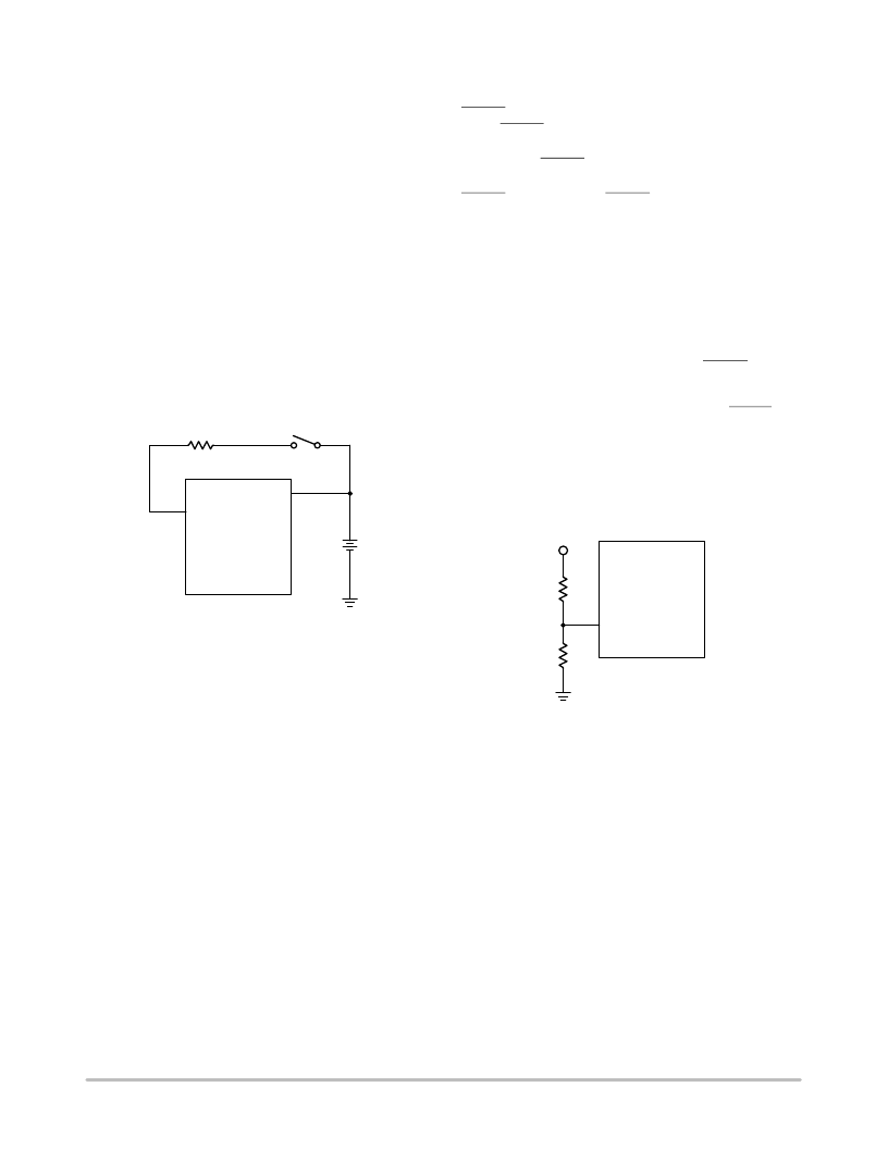
Option 2 (High Voltage). This option removes the
sequencing feature above, and allows the device to be
controlled up to the battery voltage on the ENABLE
pin with an external resistor (10 k). See Figure 5.
Figure 5. Switched Battery Application
ENABLE
V
IN
V
BAT
10 k
AUXILIARY
The AUXILIARY pin provides an alternate path for the IC
to maintain operation. The AUXILIARY pin is diode OR’d
with the V
IN
pin to the control circuitry (the DMOS output
drivers are not included). If the voltage (V
IN
) from the
battery dips as low as 3.5 V during a crank condition, the
NCV8800 will maintain operation through a 6.0 V(min)
connection on the AUXILIARY pin. Using this feature is
optional. This pin should be grounded when not in use.
V
IN
Normal supply voltage input. An external diode must be
provided to afford reverse battery protection.
SWITCH
DMOS output drivers with 0.75
max push/pull
capability. Nonoverlap logic is provided to guarantee shoot
through current is minimized.
RESET
The RESET is an open drain output which goes low when
the feedback voltage on FB1 and FB2 goes below the
undervoltage RESET threshold. The output also goes low
when the voltage on FB1 and FB2 exceeds the overvoltage
RESET threshold. The RESET output is an open drain
output capable of sinking 1.6 mA.
FB1 and FB2
FB1 and FB2 are the feedback pins to the error amplifier,
which control the output SWITCH as needed to the
regulated output. They are internally wire bonded to the
same electrical connection providing double protection for
an open circuit which would cause the buck regulator to rise
above its desired output reaching the voltage on V
IN
. These
pins also provide the feedback path for the RESET function.
DELAY
There are two options for the delay time for the RESET to go
low. Connecting the pin to GND will provide a minimum of 14
ms. Connecting the pin to FB1 and FB2 will provide a
minimum of 28 ms. Absolute max voltage on the DELAY
pin is 7.0 V. Use a resistor divider to run off higher voltages.
The 7.5 V option will require this divider (see Figure 6).
Figure 6.
DELAY
(7.0 V max)
V
OUT
COMP
The COMP pin provides access to the error amplifiers
output. Switching power supplies work as feedback control
systems, and require compensation for stability. A 1.0 k
resistor and 0.1
μ
F capacitor work well in the application in
Figure 2.
CP
The onchip DMOS drivers require the gates of the
devices to be pulled above their drain voltage. An external
capacitor located between the SWITCH output, and the CP
pin provides the charge pump action to drive the gate of the
highside driver high enough to turn the device on.
相關(guān)PDF資料 |
PDF描述 |
|---|---|
| NCV8800HDW26R2 | Synchronous Buck Regulator with 1.0 Amp Switch |
| NCV8800HDW33 | Synchronous Buck Regulator with 1.0 Amp Switch |
| NCV8800SDW26 | Synchronous Buck Regulator with 1.0 Amp Switch |
| NCV8800SDW26R2 | Synchronous Buck Regulator with 1.0 Amp Switch |
| NCV8800SDW33 | Synchronous Buck Regulator with 1.0 Amp Switch |
相關(guān)代理商/技術(shù)參數(shù) |
參數(shù)描述 |
|---|---|
| NCV8800HDW26G | 功能描述:直流/直流開關(guān)轉(zhuǎn)換器 Synchronous Buck Automotive RoHS:否 制造商:STMicroelectronics 最大輸入電壓:4.5 V 開關(guān)頻率:1.5 MHz 輸出電壓:4.6 V 輸出電流:250 mA 輸出端數(shù)量:2 最大工作溫度:+ 85 C 安裝風(fēng)格:SMD/SMT |
| NCV8800HDW26R2 | 功能描述:直流/直流開關(guān)轉(zhuǎn)換器 Synchronous Buck RoHS:否 制造商:STMicroelectronics 最大輸入電壓:4.5 V 開關(guān)頻率:1.5 MHz 輸出電壓:4.6 V 輸出電流:250 mA 輸出端數(shù)量:2 最大工作溫度:+ 85 C 安裝風(fēng)格:SMD/SMT |
| NCV8800HDW26R2G | 功能描述:直流/直流開關(guān)轉(zhuǎn)換器 Synchronous Buck Automotive RoHS:否 制造商:STMicroelectronics 最大輸入電壓:4.5 V 開關(guān)頻率:1.5 MHz 輸出電壓:4.6 V 輸出電流:250 mA 輸出端數(shù)量:2 最大工作溫度:+ 85 C 安裝風(fēng)格:SMD/SMT |
| NCV8800HDW33 | 功能描述:直流/直流開關(guān)轉(zhuǎn)換器 Synchronous Buck RoHS:否 制造商:STMicroelectronics 最大輸入電壓:4.5 V 開關(guān)頻率:1.5 MHz 輸出電壓:4.6 V 輸出電流:250 mA 輸出端數(shù)量:2 最大工作溫度:+ 85 C 安裝風(fēng)格:SMD/SMT |
| NCV8800HDW33G | 功能描述:直流/直流開關(guān)轉(zhuǎn)換器 Synchronous Buck Automotive RoHS:否 制造商:STMicroelectronics 最大輸入電壓:4.5 V 開關(guān)頻率:1.5 MHz 輸出電壓:4.6 V 輸出電流:250 mA 輸出端數(shù)量:2 最大工作溫度:+ 85 C 安裝風(fēng)格:SMD/SMT |
發(fā)布緊急采購(gòu),3分鐘左右您將得到回復(fù)。