- 您現在的位置:買賣IC網 > PDF目錄361100 > NCP400FCT2G (ON SEMICONDUCTOR) 150 mA CMOS Low Iq Low-Dropout Voltage Regulator with Voltage Detector Output PDF資料下載
參數資料
| 型號: | NCP400FCT2G |
| 廠商: | ON SEMICONDUCTOR |
| 元件分類: | 基準電壓源/電流源 |
| 英文描述: | 150 mA CMOS Low Iq Low-Dropout Voltage Regulator with Voltage Detector Output |
| 中文描述: | 1.8 V FIXED POSITIVE LDO REGULATOR, 0.2 V DROPOUT, PBGA6 |
| 封裝: | LEAD FREE, FCP-6 |
| 文件頁數: | 9/14頁 |
| 文件大小: | 106K |
| 代理商: | NCP400FCT2G |
NCP400
http://onsemi.com
9
OPERATION DESCRIPTION
Low Dropout Voltage Regulator
The low dropout voltage regulator contains a voltage
reference unit, an error amplifier, a PMOS power transistor,
resistors for setting output voltage, current limit and thermal
shutdown protection circuits.
Enable Operation
The enable pin will turn on or off the regulator. The limits
of threshold are covered in the electrical specification
section of this data sheet. If the enable is not used then the
pin should be connected to V
in
.
Voltage Detector
The NCP400 consist of a precision voltage detector that
drives a time delay generator. Figures 23 and 24 show a
timing diagram and a typical application. Initially consider
that input voltage V
in
is at a nominal level and it is greater
than the voltage detector upper threshold (V
DET+
). The
voltage at CD Pin (Pin 4) will be at the same level as Vin, and
the reset output (Pin 3) will be in the high state. If there is a
power interruption and Vin becomes significantly deficient,
it will fall below the lower detector threshold (V
DET
) and
the external time delay capacitor CD will be immediately
discharged by an internal NChannel MOSFET that
connects to Pin 4. This sequence of events causes the Reset
output to be in the low state. After completion of the power
interruption, V
in
will again return to its nominal level and
become greater than the V
DET+
. The voltage detector will
turn off the NChannel MOSFET and allow internal current
source to charge the external capacitor CD, thus creating a
programmable delay for releasing the reset signal. When the
voltage at CD Pin 4 exceeds the inverter threshold, typically
0.97 V, the reset output will revert back to its original state.
The detail reset output time delay calculation is shown in
Figure 24.
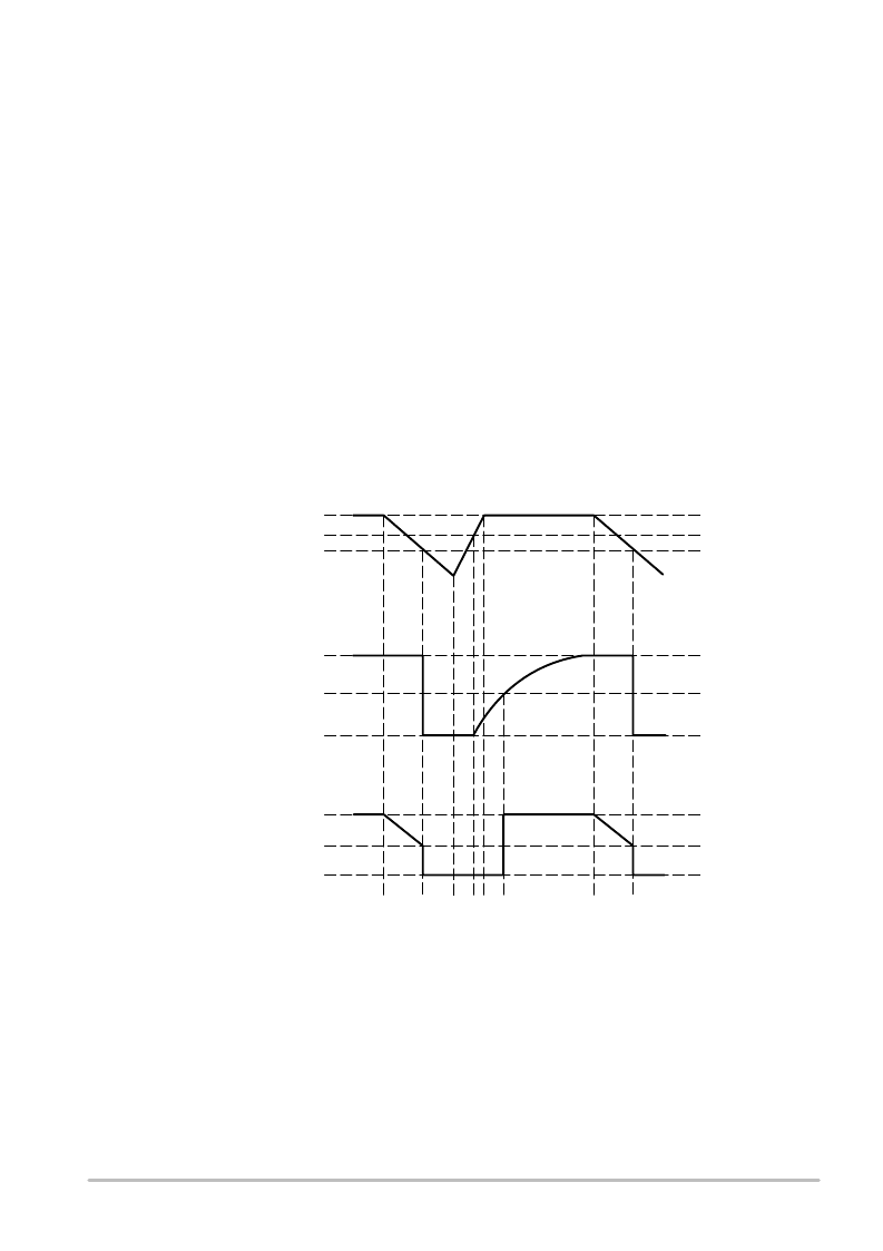
Figure 23. Timing diagram
V
in
V
DET+
V
DET
V
in
V
DET
V
in
0.97 V
0 V
Capacitor, Pin 4
Reset Output, Pin 3
Input Voltage, Pin 1
相關PDF資料 |
PDF描述 |
|---|---|
| NCP4326DR2 | Secondary Controller for Multi−Output Quasi−Resonant Switchmode Power Supplies |
| NCP4326DR2G | Secondary Controller for Multi−Output Quasi−Resonant Switchmode Power Supplies |
| NCP4330DR2G | Post Regulation Driver |
| NCP4330 | 300 W 80 PLUS ATX Reference Design |
| NCP4331DR2G | Synchronous Buck Controller for High Efficiency Post Regulation |
相關代理商/技術參數 |
參數描述 |
|---|---|
| NCP4115AVKR2 | 制造商:Rochester Electronics LLC 功能描述:- Bulk |
| NCP4115VKR2 | 功能描述:監(jiān)控電路 ANA PMU RoHS:否 制造商:STMicroelectronics 監(jiān)測電壓數: 監(jiān)測電壓: 欠電壓閾值: 過電壓閾值: 輸出類型:Active Low, Open Drain 人工復位:Resettable 監(jiān)視器:No Watchdog 電池備用開關:No Backup 上電復位延遲(典型值):10 s 電源電壓-最大:5.5 V 最大工作溫度:+ 85 C 安裝風格:SMD/SMT 封裝 / 箱體:UDFN-6 封裝:Reel |
| NCP4200 | 制造商:ONSEMI 制造商全稱:ON Semiconductor 功能描述:Programmable Multi-Phase Synchronous Buck Converter with PMBus |
| NCP4200MNR2G | 功能描述:DC/DC 開關控制器 VR11.1 4PH CTRL PMBUS ITF RoHS:否 制造商:Texas Instruments 輸入電壓:6 V to 100 V 開關頻率: 輸出電壓:1.215 V to 80 V 輸出電流:3.5 A 輸出端數量:1 最大工作溫度:+ 125 C 安裝風格: 封裝 / 箱體:CPAK |
| NCP4201MNR2G | 功能描述:直流/直流開關轉換器 VR11.1 4PH CTRL PMBUS ITF RoHS:否 制造商:STMicroelectronics 最大輸入電壓:4.5 V 開關頻率:1.5 MHz 輸出電壓:4.6 V 輸出電流:250 mA 輸出端數量:2 最大工作溫度:+ 85 C 安裝風格:SMD/SMT |
發(fā)布緊急采購,3分鐘左右您將得到回復。