- 您現(xiàn)在的位置:買賣IC網(wǎng) > PDF目錄361089 > NCP1013 (ON SEMICONDUCTOR) Self-Supplied Monolithic Switcher for Low Standby- Power Offline SMPS PDF資料下載
參數(shù)資料
| 型號(hào): | NCP1013 |
| 廠商: | ON SEMICONDUCTOR |
| 英文描述: | Self-Supplied Monolithic Switcher for Low Standby- Power Offline SMPS |
| 中文描述: | 自提供的單片切換為低待機(jī)功耗離線開關(guān)電源 |
| 文件頁(yè)數(shù): | 17/24頁(yè) |
| 文件大?。?/td> | 324K |
| 代理商: | NCP1013 |
第1頁(yè)第2頁(yè)第3頁(yè)第4頁(yè)第5頁(yè)第6頁(yè)第7頁(yè)第8頁(yè)第9頁(yè)第10頁(yè)第11頁(yè)第12頁(yè)第13頁(yè)第14頁(yè)第15頁(yè)第16頁(yè)當(dāng)前第17頁(yè)第18頁(yè)第19頁(yè)第20頁(yè)第21頁(yè)第22頁(yè)第23頁(yè)第24頁(yè)
NCP1010, NCP1011, NCP1012, NCP1013, NCP1014
http://onsemi.com
17
Design Procedure
The design of an SMPS around a monolithic device does
not differ from that of a standard circuit using a controller
and a MOSFET. However, one needs to be aware of certain
characteristics specific of monolithic devices:
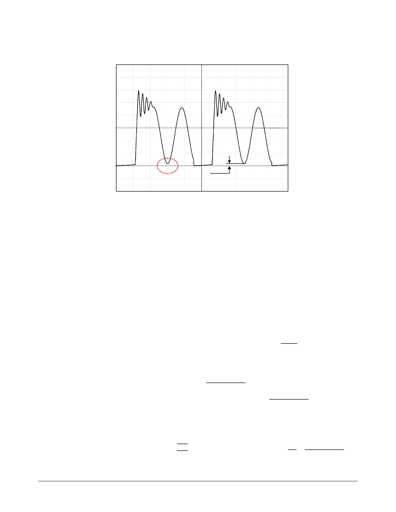
Figure 26. The DrainSource Wave Shall Always be Positive . . .
1.004M
1.011M
1.018M
1.025M
1.032M
50.0
50.0
150
250
350
> 0 !!
1. In any case, the lateral MOSFET bodydiode shall
never be forward biased, either during startup
(because of a large leakage inductance) or in
normal operation as shown by Figure 26.
As a result, the Flyback voltage which is reflected on the
drain at the switch opening cannot be larger than the input
voltage. When selecting components, you thus must adopt
a turn ratio which adheres to the following equation:
N · (Vout
Vf)
Vinmin
operating from a 120 V DC rail, with a delivery of 12 V, we
can select a reflected voltage of 100 Vdc maximum:
120–100 > 0. Therefore, the turn ratio Np:Ns must be
smaller than 100/(12 + 1) = 7.7 or Np:Ns < 7.7. We will see
later on how it affects the calculation.
2. A currentmode architecture is, by definition,
sensitive to subharmonic oscillations.
Subharmonic oscillations only occur when the
SMPS is operating in Continuous Conduction
Mode (CCM) together with a dutycycle greater
than 50%. As a result, we recommend to operate
the device in DCM only, whatever dutycycle it
implies (max = 65%). However, CCM operation
with dutycycles below 40% is possible.
3. Lateral MOSFETs have a poorly dopped
bodydiode which naturally limits their ability to
sustain the avalanche. A traditional RCD clamping
network shall thus be installed to protect the
MOSFET. In some low power applications,
a simple capacitor can also be used since
(eq. 14)
. For instance, if
Vdrain max
Vin
N · (Vout
Vf)
Ip ·
Lf
Ctot
(eq. 15)
, where Lf is the leakage inductance,
Ctot is the total capacitance at the drain node
(which is increased by the capacitor wired between
drain and source), N the Np:Ns turn ratio, Vout the
output voltage, Vf the secondary diode forward
drop and finally, Ip the maximum peak current.
Worse case occurs when the SMPS is very close to
regulation, e.g. the Vout target is almost reached
and Ip is still pushed to the maximum.
Taking into account all previous remarks, it becomes
possible to calculate the maximum power that can be
transferred at low line.
When the switch closes, Vin is applied across the primary
inductance Lp until the current reaches the level imposed by
the feedback loop. The duration of this event is called the ON
time and can be defined by:
Lp · Ip
ton
Vin
(eq. 16)
At the switch opening, the primary energy is transferred
to the secondary and the flyback voltage appears across
Lp, resetting the transformer core with a slope of
N · (Vout
Vf)
Lp
Lp · Ip
N · (Vout
If one wants to keep DCM only, but still need to pass the
maximum power, we will not allow a deadtime after the
core is reset, but rather immediately restart. The switching
time can be expressed by:
. toff, the OFF time is thus:
toff
Vf)
(eq. 17)
Tsw
toff
ton
Lp · Ip ·
1
Vin
1
N · (Vout
Vf)
(eq. 18)
相關(guān)PDF資料 |
PDF描述 |
|---|---|
| NCP1014 | Self-Supplied Monolithic Switcher for Low Standby- Power Offline SMPS |
| NCP1014APL100R2 | Self-Supplied Monolithic Switcher for Low Standby- Power Offline SMPS |
| NCP1012APL130R2 | Self-Supplied Monolithic Switcher for Low Standby- Power Offline SMPS |
| NCP1010ST100T3 | 24 Characters x 2 Lines, 5x7 Dot Matrix Character and Cursor |
| NCP1010ST130T3 | 24 Characters x 2 Lines, 5x7 Dot Matrix Character and Cursor |
相關(guān)代理商/技術(shù)參數(shù) |
參數(shù)描述 |
|---|---|
| NCP1013/D | 制造商:未知廠家 制造商全稱:未知廠家 功能描述:Self-Supplied Monolithic Switcher for Low Standby-Power Offline SMPS |
| NCP1013ADAPGEVB | 功能描述:電源管理IC開發(fā)工具 NCP1013 6/12W ADAPTER EVB RoHS:否 制造商:Maxim Integrated 產(chǎn)品:Evaluation Kits 類型:Battery Management 工具用于評(píng)估:MAX17710GB 輸入電壓: 輸出電壓:1.8 V |
| NCP1013AP065 | 功能描述:電流型 PWM 控制器 Low Standby Power RoHS:否 制造商:Texas Instruments 開關(guān)頻率:27 KHz 上升時(shí)間: 下降時(shí)間: 工作電源電壓:6 V to 15 V 工作電源電流:1.5 mA 輸出端數(shù)量:1 最大工作溫度:+ 105 C 安裝風(fēng)格:SMD/SMT 封裝 / 箱體:TSSOP-14 |
| NCP1013AP065G | 功能描述:電流型 PWM 控制器 Low Standby Power Monolithic Switcher RoHS:否 制造商:Texas Instruments 開關(guān)頻率:27 KHz 上升時(shí)間: 下降時(shí)間: 工作電源電壓:6 V to 15 V 工作電源電流:1.5 mA 輸出端數(shù)量:1 最大工作溫度:+ 105 C 安裝風(fēng)格:SMD/SMT 封裝 / 箱體:TSSOP-14 |
| NCP1013AP100 | 功能描述:電流型 PWM 控制器 Low Standby Power RoHS:否 制造商:Texas Instruments 開關(guān)頻率:27 KHz 上升時(shí)間: 下降時(shí)間: 工作電源電壓:6 V to 15 V 工作電源電流:1.5 mA 輸出端數(shù)量:1 最大工作溫度:+ 105 C 安裝風(fēng)格:SMD/SMT 封裝 / 箱體:TSSOP-14 |
發(fā)布緊急采購(gòu),3分鐘左右您將得到回復(fù)。