- 您現(xiàn)在的位置:買賣IC網(wǎng) > PDF目錄9501 > NBXSPA022LN1TAG (ON Semiconductor)IC CLK XO LVPECL 187.5MHZ 6CLCC PDF資料下載
參數(shù)資料
| 型號: | NBXSPA022LN1TAG |
| 廠商: | ON Semiconductor |
| 文件頁數(shù): | 4/6頁 |
| 文件大小: | 0K |
| 描述: | IC CLK XO LVPECL 187.5MHZ 6CLCC |
| 產(chǎn)品培訓(xùn)模塊: | XO Replacement Overview |
| 標(biāo)準(zhǔn)包裝: | 1 |
| 系列: | PureEdge™ |
| 類型: | 振蕩器 - 晶體 |
| 頻率: | 187.5MHz |
| 電源電壓: | 2.375 V ~ 3.63 V |
| 電流 - 電源: | 85mA |
| 工作溫度: | -40°C ~ 85°C |
| 封裝/外殼: | 6-CLCC |
| 包裝: | 標(biāo)準(zhǔn)包裝 |
| 供應(yīng)商設(shè)備封裝: | 6-CLCC(7x5) |
| 安裝類型: | 表面貼裝 |
| 其它名稱: | NBXSPA022LN1TAGOSDKR |
NBXSPA022
http://onsemi.com
4
Table 6. AC CHARACTERISTICS (VDD = 2.5 V ± 5% or VDD = 3.3 V ± 10%, GND = 0 V, TA = 40°C to +85°C) (Note 4)
Symbol
Characteristic
Conditions
Min.
Typ.
Max.
Units
fCLKOUT
Output Clock Frequency
187.5
MHz
Df
Frequency Stability NBXSPA022
(Note 5)
±50
ppm
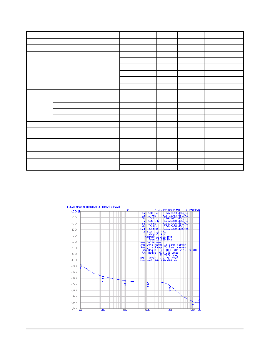
FNOISE
PhaseNoise Performance
100 Hz of Carrier
96
dBc/Hz
fCLKout = 187.5 MHz
(See Figure 3)
1 kHz of Carrier
117
dBc/Hz
10 kHz of Carrier
124
dBc/Hz
100 kHz of Carrier
126
dBc/Hz
1 MHz of Carrier
133
dBc/Hz
10 MHz of Carrier
158
dBc/Hz
tjit(F)
RMS Phase Jitter
12 kHz to 20 MHz
0.5
0.75
ps
tjitter
Cycle to Cycle, RMS
1000 Cycles
1
8
ps
Cycle to Cycle, PeaktoPeak
1000 Cycles
7
35
ps
Period, RMS
10,000 Cycles
0.6
4
ps
Period, PeaktoPeak
10,000 Cycles
5
20
ps
tOE/OD
Output Enable/Disable Time
200
ns
tDUTY_CYCLE
Output Clock Duty Cycle
(Measured at Cross Point)
48
50
52
%
tR
Output Rise Time (20% and 80%)
250
400
ps
tF
Output Fall Time (80% and 20%)
250
400
ps
tstart
Startup Time
1
5
ms
Aging
1st Year
3
ppm
Every Year After 1st
1
ppm
NOTE: Device will meet the specifications after thermal equilibrium has been established when mounted in a test socket or printed circuit
board with maintained transverse airflow greater than 500 Ifpm. Electrical parameters are guaranteed only over the declared
operating temperature range. Functional operation of the device exceeding these conditions is not implied. Device specification limit
values are applied individually under normal operating conditions and not valid simultaneously.
4. Measurement taken with outputs terminated with 100 ohm across differential pair. See Figure 4.
5. Parameter guarantees 10 years of aging. Includes initial stability at 25°C, shock, vibration and first year aging.
Figure 3. Typical Phase Noise Plot at 187.5 MHz
相關(guān)PDF資料 |
PDF描述 |
|---|---|
| V110A36M300BF2 | CONVERTER MOD DC/DC 36V 300W |
| NBXSBA031LN1TAG | IC CLK XO LVPECL 340.00MHZ 6CLCC |
| MS27467T25B20SA | CONN PLUG 30POS STRAIGHT W/SCKT |
| MS27468P25B1S | CONN RCPT 128POS JAM NUT W/SCKT |
| CS3106A-22-77S | CONN PLUG 14POS STRAIGHT W/SCKT |
相關(guān)代理商/技術(shù)參數(shù) |
參數(shù)描述 |
|---|---|
| NBXSPA022LNHTAG | 功能描述:標(biāo)準(zhǔn)時鐘振蕩器 XO LVDS 187.7500 MHZ RoHS:否 制造商:AVX 產(chǎn)品:Standard Clock Oscillators 封裝 / 箱體:7 mm x 5 mm 頻率:75 MHz 頻率穩(wěn)定性:50 PPM 電源電壓:2.5 V 負(fù)載電容: 端接類型:SMD/SMT 最小工作溫度:0 C 最大工作溫度:+ 70 C 輸出格式:LVDS 尺寸: 封裝:Reel 系列: |
| NBXSPA022LU1TAG | 功能描述:標(biāo)準(zhǔn)時鐘振蕩器 3.3V LVPECL Network GigE RoHS:否 制造商:AVX 產(chǎn)品:Standard Clock Oscillators 封裝 / 箱體:7 mm x 5 mm 頻率:75 MHz 頻率穩(wěn)定性:50 PPM 電源電壓:2.5 V 負(fù)載電容: 端接類型:SMD/SMT 最小工作溫度:0 C 最大工作溫度:+ 70 C 輸出格式:LVDS 尺寸: 封裝:Reel 系列: |
| NC 051 | 制造商:Thomas & Betts 功能描述:1 1/2" CONN,CLMP,NMSC,DC,NON-WTRTT ;ROHS COMPLIANT: YES 制造商:Thomas & Betts 功能描述:Cable Clamps and Clips Clamp Zinc Die Cast |
| NC 061 | 制造商:Thomas & Betts 功能描述:2" CONN,CLMP,NMSC,DC,NON-WTRTT 制造商:Thomas & Betts 功能描述:Fittings Clamp 2inch Zinc |
| NC 201 | 制造商:Thomas & Betts 功能描述:3/8" CONN,NM CLMP,USE W/ NMSC,DC 制造商:Thomas & Betts 功能描述:Fittings Clamp 0.375inch Zinc |
發(fā)布緊急采購,3分鐘左右您將得到回復(fù)。