- 您現(xiàn)在的位置:買賣IC網(wǎng) > PDF目錄385645 > MXSMCGLCE10A (MICROSEMI CORP) 1500 WATT LOW CAPACITANCE SURFACE MOUNT TRANSIENT VOLTAGE SUPPRESSOR PDF資料下載
參數(shù)資料
| 型號(hào): | MXSMCGLCE10A |
| 廠商: | MICROSEMI CORP |
| 元件分類: | 參考電壓二極管 |
| 英文描述: | 1500 WATT LOW CAPACITANCE SURFACE MOUNT TRANSIENT VOLTAGE SUPPRESSOR |
| 中文描述: | 1500 W, UNIDIRECTIONAL, SILICON, TVS DIODE, DO-215AB |
| 封裝: | PLASTIC, SMCG, 2 PIN |
| 文件頁(yè)數(shù): | 1/4頁(yè) |
| 文件大小: | 168K |
| 代理商: | MXSMCGLCE10A |
1500 WATT LOW CAPACITANCE
SURFACE MOUNT TRANSIENT
VOLTAGE SUPPRESSOR
W
M
.
C
SCOTTSDALE
DIVISION
SMCGLCE6.5 thru SMCGLCE170A, e3
SMCJLCE6.5 thru SMCJLCE170A, e3
S
L
DES CRIPT ION
APPEARANCE
This surface mount Transient Voltage Suppressor (TVS) product family includes a
rectifier diode element in series and opposite direction to achieve low capacitance
below 100 pF. They are also available as RoHS Compliant with an e3 suffix. The low
TVS capacitance may be used for protecting higher frequency applications in inductive
switching environments or electrical systems involving secondary lightning effects per
IEC61000-4-5 as well as RTCA/DO-160D or ARINC 429 for airborne avionics. They
also protect from ESD and EFT per IEC61000-4-2 and IEC61000-4-4. If bipolar
transient capability is required, two of these low capacitance TVS devices may be used
in parallel and opposite directions (anti-parallel) for complete ac protection (Figure 6).
IMPORTANT:
For the most current data, consult
MICROSEMI’s
website:
http://www.microsemi.com
FEAT URES
APPLICAT IONS / BENEFITS
Available in standoff voltage range of 6.5 to 200 V
Low capacitance of 100 pF or less
Molding compound flammability rating: UL94V-O
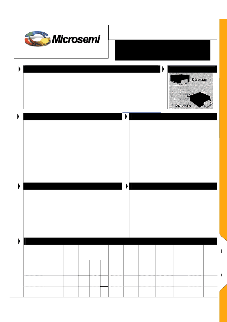
Two different terminations available in C-bend (modified J-
Bend with DO-214AB) or Gull-wing (DO-215AB)
Options for screening in accordance with MIL-PRF-19500
for JAN, JANTX, JANTXV, and JANS are available by
adding MQ, MX, MV, or MSP prefixes respectively to part
numbers
Optional 100% screening for avionics grade is available by
adding MA prefix to part number for 100% temperature
cycle –55oC to 125oC (10X) as well as surge (3X) and 24
hours HTRB with post test V
BR
& I
R
RoHS Compliant devices available by adding an “e3” suffix
MAX IMUM RATINGS
1500 Watts of Peak Pulse Power dissipation at 25
o
C
with
repetition rate of 0.01% or less*
Clamping Factor: 1.4 @ Full Rated power
1.30 @ 50% Rated power
t
clamping
(0 volts to V
(BR)
min): Less than 5x10
-9
seconds
Operating and Storage temperatures: -65 to +150
C
Steady State power dissipation: 5.0W @ T
L
= 50
o
C
THERMAL RESISTANCE: 20
o
C/W (typical junction to
lead (tab) at mounting plane
* When pulse testing, do not pulse in opposite direction
(see “Schematic Applications” section herein and
Figures 5 & 6 for further protection in both directions)
1500 Watts of Peak Pulse Power at 10/1000
μ
s
Protection for aircraft fast data rate lines per select
level waveforms in RTCA/DO-160D & ARINC 429
Low capacitance for high speed data line
interfaces
IEC61000-4-2 ESD 15 kV (air), 8 kV (contact)
IEC61000-4-5 (Lightning) as further detailed in
LCE6.5 thru LCE170A data sheet
T1/E1 Line Cards
Base Stations
WAN Interfaces
XDSL Interfaces
CSU/DSU Equipment
MECHANICAL AND PACK AGING
CASE: Molded, surface mountable
TERMINALS: Gull-wing or C-bend (modified J-
bend) tin-lead or RoHS compliant annealed
matte-tin plating solderable per MIL-STD-750,
method 2026
POLARITY: Cathode indicated by band
MARKING: Part number without prefix (e.g.
LCE6.5A, LCE6.5Ae3, LCE33, LCE33Ae3, etc.
TAPE & REEL option: Standard per EIA-481-B
with 16 mm tape, 750 per 7 inch reel or 2500 per
13 inch reel (add “TR” suffix to part number)
ELECT RICAL CHARACT ERIS T ICS @ 25
o
C
Breakdown Voltage
V
BR
@ I
(BR)
Volts
MICROSEMI
Part Number
Gull-Wing
“G”
Bend Lead
SMCGLCE6.5
SMCGLCE6.5A
SMCGLCE7.0
SMCGLCE7.0A
SMCGLCE7.5
SMCGLCE7.5A
SMCGLCE8.0
SMCGLCE8.0A
SMCGLCE8.5
SMCGLCE8.5A
SMCGLCE9.0
SMCGLCE9.0A
MICROSEMI
Part Number
Modified
“J”
Bend Lead
SMCJLCE6.5
SMCJLCE6.5A
SMCJLCE7.0
SMCJLCE7.0A
SMCJLCE7.5
SMCJLCE7.5A
SMCJLCE8.0
SMCJLCE8.0A
SMCJLCE8.5
SMCJLCE8.5A
SMCJLCE9.0
SMCJLCE9.0A
Reverse
Stand-Off
Voltage
V
WM
Volts
6.5
6.5
7.0
7.0
7.5
7.5
8.0
8.0
8.5
8.5
9.0
9.0
MIN
7.22
7.22
7.78
7.78
8.33
8.33
8.89
8.89
9.44
9.44
10.0
10.0
MAX
8.82
7.98
9.51
8.60
10.2
9.21
10.9
9.83
11.5
10.4
12.2
11.1
mA
10
10
10
10
10
10
1
1
1
1
1
1
Maximum
Reverse
Leakage
@V
WM
I
D
μ
A
1000
1000
500
500
250
250
100
100
50
50
10
10
Maximum
Clamping
Voltage
@I
PP
V
Volts
12.3
11.2
13.3
12.0
14.3
12.9
15.0
13.6
15.9
14.4
16.9
15.4
Maximum
Peak Pulse
Current
I
PP
@10/1000
Amps
100
100
100
100
100
100
100
100
94
100
89
97
Maximum
Capacitance
@ 0 Volts,
f = 1 MHz
pF
75
75
75
75
100
100
100
100
100
100
100
100
V
WIB
Working
Inverse
Blocking
Voltage
Volts
75
75
75
75
75
75
75
75
75
75
75
75
Microsemi
Scottsdale Division
Page 1
I
IB
Inverse
Blocking
Leakage
Current
mA
1
1
1
1
1
1
1
1
1
1
1
1
V
PIB
Peak
Inverse
Blocking
Voltage
Volts
100
100
100
100
100
100
100
100
100
100
100
100
Copyright
2005
6-06-2005 REV D
8700 E. Thomas Rd. PO Box 1390, Scottsdale, AZ 85252 USA, (480) 941-6300, Fax: (480) 947-1503
相關(guān)PDF資料 |
PDF描述 |
|---|---|
| MXSMCGLCE10ATR | 1500 WATT LOW CAPACITANCE SURFACE MOUNT TRANSIENT VOLTAGE SUPPRESSOR |
| MXSMCGLCE10TR | 1500 WATT LOW CAPACITANCE SURFACE MOUNT TRANSIENT VOLTAGE SUPPRESSOR |
| MXSMCGLCE11 | 1500 WATT LOW CAPACITANCE SURFACE MOUNT TRANSIENT VOLTAGE SUPPRESSOR |
| MXSMCGLCE110 | 1500 WATT LOW CAPACITANCE SURFACE MOUNT TRANSIENT VOLTAGE SUPPRESSOR |
| MXSMCGLCE110A | 1500 WATT LOW CAPACITANCE SURFACE MOUNT TRANSIENT VOLTAGE SUPPRESSOR |
相關(guān)代理商/技術(shù)參數(shù) |
參數(shù)描述 |
|---|---|
| MXSMCGLCE10AE3 | 制造商:Microsemi Corporation 功能描述:TRANSIENT VOLTAGE SUPPRESSOR - Bulk |
| MXSMCGLCE10ATR | 制造商:MICROSEMI 制造商全稱:Microsemi Corporation 功能描述:1500 WATT LOW CAPACITANCE SURFACE MOUNT TRANSIENT VOLTAGE SUPPRESSOR |
| MXSMCGLCE10TR | 制造商:MICROSEMI 制造商全稱:Microsemi Corporation 功能描述:1500 WATT LOW CAPACITANCE SURFACE MOUNT TRANSIENT VOLTAGE SUPPRESSOR |
| MXSMCGLCE11 | 制造商:MICROSEMI 制造商全稱:Microsemi Corporation 功能描述:1500 WATT LOW CAPACITANCE SURFACE MOUNT TRANSIENT VOLTAGE SUPPRESSOR |
| MXSMCGLCE110 | 制造商:MICROSEMI 制造商全稱:Microsemi Corporation 功能描述:1500 WATT LOW CAPACITANCE SURFACE MOUNT TRANSIENT VOLTAGE SUPPRESSOR |
發(fā)布緊急采購(gòu),3分鐘左右您將得到回復(fù)。