- 您現(xiàn)在的位置:買賣IC網(wǎng) > PDF目錄371153 > MTY25N60E (MOTOROLA INC) TMOS POWER FET 25 AMPERES 600 VOLTS RDS(on) = 0.21 OHM PDF資料下載
參數(shù)資料
| 型號: | MTY25N60E |
| 廠商: | MOTOROLA INC |
| 元件分類: | JFETs |
| 英文描述: | TMOS POWER FET 25 AMPERES 600 VOLTS RDS(on) = 0.21 OHM |
| 中文描述: | 25 A, 600 V, 0.21 ohm, N-CHANNEL, Si, POWER, MOSFET, TO-264AA |
| 封裝: | TO-264, 3 PIN |
| 文件頁數(shù): | 2/8頁 |
| 文件大小: | 236K |
| 代理商: | MTY25N60E |
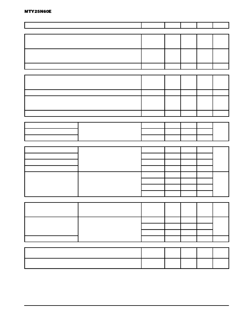
2
Motorola TMOS Power MOSFET Transistor Device Data
ELECTRICAL CHARACTERISTICS
(TJ = 25
°
C unless otherwise noted)
Characteristic
Symbol
Min
Typ
Max
Unit
OFF CHARACTERISTICS
Drain–Source Breakdown Voltage
(VGS = 0, ID = 250
μ
A)
Temperature Coefficient (Positive)
V(BR)DSS
600
—
—
714
—
—
Vdc
mV/
°
C
Zero Gate Voltage Drain Current
(VDS = 600 Vdc, VGS = 0 Vdc)
(VDS = 600 Vdc, VGS = 0 Vdc, TJ = 125
°
C)
Gate–Body Leakage Current (VGS =
±
20 Vdc, VDS = 0)
IDSS
—
—
—
—
10
200
μ
Adc
IGSS
—
—
100
nAdc
ON CHARACTERISTICS (1)
Gate Threshold Voltage
(VDS = VGS, ID = 250
μ
Adc)
Threshold Temperature Coefficient (Negative)
VGS(th)
2
—
—
7
4
—
Vdc
mV/
°
C
Static Drain–Source On–Resistance (VGS = 10 Vdc, ID = 12.5 Adc)
Drain–Source On–Voltage (VGS = 10 Vdc)
(ID = 25 Adc)
(ID = 12.5 Adc, TJ = 125
°
C)
RDS(on)
VDS(on)
—
—
0.21
Ohm
—
—
5.2
—
6
7
Vdc
Forward Transconductance (VDS = 15 Vdc, ID = 12.5 Adc)
gFS
18
—
—
mhos
DYNAMIC CHARACTERISTICS
Input Capacitance
f = 1.0 MHz)
Ciss
Coss
Crss
—
7300
10220
pF
Output Capacitance
(VDS = 25 Vdc, VGS = 0 Vdc,
—
700
1100
Reverse Transfer Capacitance
—
110
250
SWITCHING CHARACTERISTICS (2)
Turn–On Delay Time
)
RG = 4.7
td(on)
tr
td(off)
tf
—
32
60
ns
Rise Time
(VDD = 300 Vdc, ID = 25 Adc,
VGS = 10 Vdc,
—
90
175
Turn–Off Delay Time
—
170
300
Fall Time
—
110
200
Gate Charge
(See Figure 8)
VGS = 10 Vdc)
QT
Q1
Q2
Q3
—
240
350
nC
(VDS = 480 Vdc, ID = 25 Adc,
—
30
—
—
110
—
—
65
—
SOURCE–DRAIN DIODE CHARACTERISTICS
Forward On–Voltage
(IS = 25 Adc, VGS = 0 Vdc)
(IS = 25 Adc, VGS = 0 Vdc, TJ = 125
°
C)
VSD
—
—
0.9
0.8
1.2
—
Vdc
Reverse Recovery Time
(See Figure 14)
dIS/dt = 100 A/
μ
s)
trr
—
620
—
ns
(IS = 25 Adc, VGS = 0 Vdc,
ta
tb
—
310
—
—
310
—
Reverse Recovery Stored Charge
QRR
—
10.42
—
μ
C
INTERNAL PACKAGE INDUCTANCE
Internal Drain Inductance
(Measured from the drain lead 0.25
″
from package to center of die)
LD
—
4.5
—
nH
Internal Source Inductance
(Measured from the source lead 0.25
″
from package to source bond pad)
LS
—
7.5
—
nH
(1) Pulse Test: Pulse Width
≤
300
μ
s, Duty Cycle
≤
2%.
(2) Switching characteristics are independent of operating junction temperature.
相關PDF資料 |
PDF描述 |
|---|---|
| MTY30N50 | TMOS POWER FET 30 AMPERES 500 VOLTS RDS(on) = 0.15 OHM |
| MTY30N50E | TMOS POWER FET 30 AMPERES 500 VOLTS RDS(on) = 0.15 OHM |
| MTY55N20E | TMOS POWER FET 55 AMPERES 200 VOLTS RDS(on) = 0.028 OHM |
| MU82 | 8-input to 1-output digital multiplexer with 2x drive strength |
| MUN5111T1 | EMITTER IR 880NM T0-18 |
相關代理商/技術參數(shù) |
參數(shù)描述 |
|---|---|
| MTY300A | 制造商:LIUJING 制造商全稱:LIUJING 功能描述:可控硅、晶閘管 |
| MTY30N50 | 制造商:MOTOROLA 制造商全稱:Motorola, Inc 功能描述:TMOS POWER FET 30 AMPERES 500 VOLTS RDS(on) = 0.15 OHM |
| MTY30N50E | 制造商:Rochester Electronics LLC 功能描述:- Bulk 制造商:ON Semiconductor 功能描述: |
| MTY55N20E | 制造商:MOTOROLA 制造商全稱:Motorola, Inc 功能描述:TMOS POWER FET 55 AMPERES 200 VOLTS RDS(on) = 0.028 OHM |
| MTZ.0S.045.065 | 制造商:LEMO connectors 功能描述: |
發(fā)布緊急采購,3分鐘左右您將得到回復。