- 您現(xiàn)在的位置:買(mǎi)賣(mài)IC網(wǎng) > PDF目錄224505 > MSP58C20 (Texas Instruments, Inc.) Audio-Band Converter PDF資料下載
參數(shù)資料
| 型號(hào): | MSP58C20 |
| 廠商: | Texas Instruments, Inc. |
| 英文描述: | Audio-Band Converter |
| 中文描述: | 語(yǔ)音頻帶轉(zhuǎn)換器 |
| 文件頁(yè)數(shù): | 15/17頁(yè) |
| 文件大?。?/td> | 298K |
| 代理商: | MSP58C20 |
第1頁(yè)第2頁(yè)第3頁(yè)第4頁(yè)第5頁(yè)第6頁(yè)第7頁(yè)第8頁(yè)第9頁(yè)第10頁(yè)第11頁(yè)第12頁(yè)第13頁(yè)第14頁(yè)當(dāng)前第15頁(yè)第16頁(yè)第17頁(yè)
MSP58C20
AUDIO-BAND CONVERTER
SPSS015B – DECEMBER 1993 – REVISED JULY 1996
7
POST OFFICE BOX 655303
DALLAS, TEXAS 75265
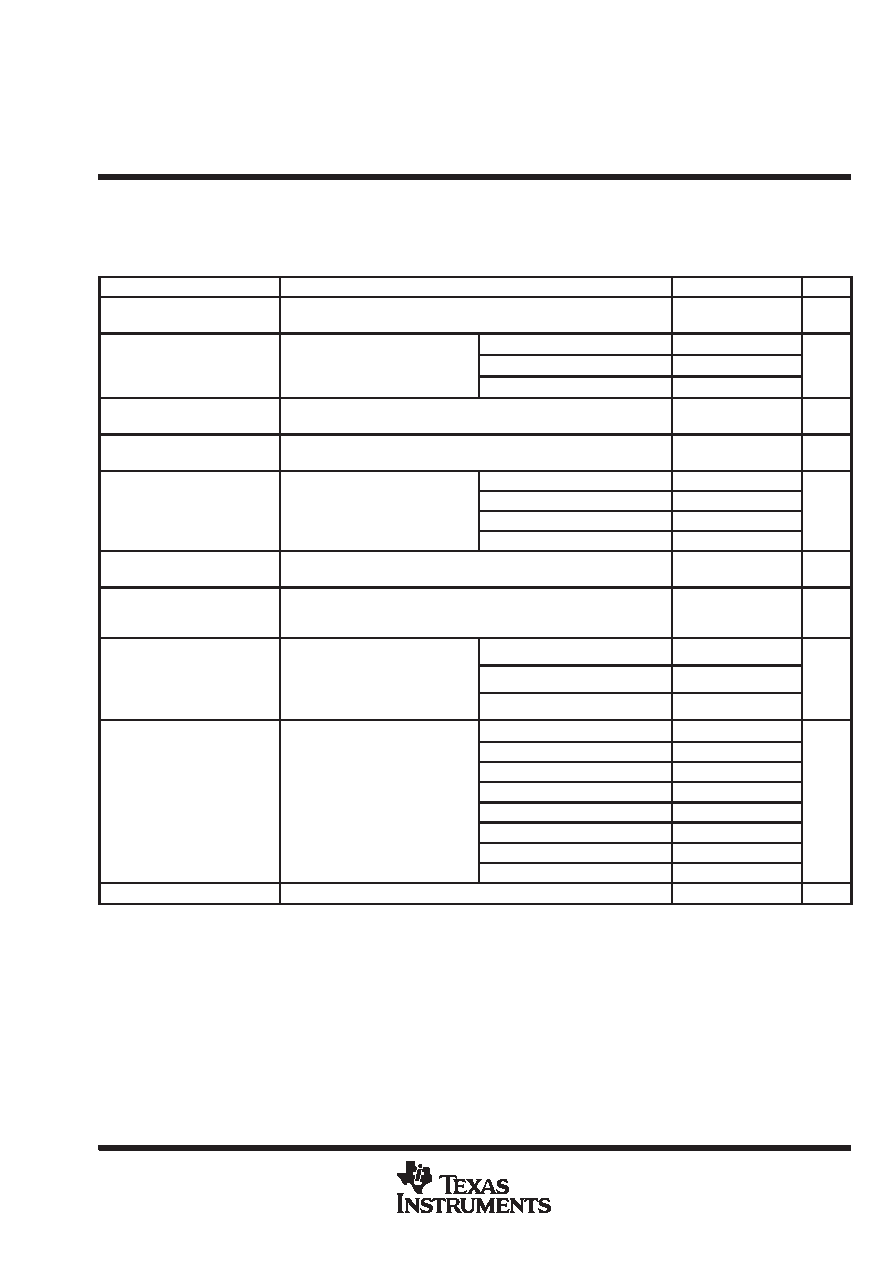
electrical characteristics over recommended ranges of supply voltage and operating free-air
temperature, ADCLK input frequency = 1.024 MHz, PWDA = L and PWAD = L (power-up mode)
(unless otherwise noted) (continued)
DAC receive characteristics
PARAMETER
TEST CONDITIONS
MIN
TYP
MAX
UNIT
Receive gain tolerance
VDD = 5 V,
TA = 25°C,
Input = 1-kHz sine wave at – 28 dBrl
±0.5
dB
Input = 1-kHz sine wave,
Gi
f
l
i
Input level = – 1 dBrl to – 43 dBrl
±0.25
Receive gain versus input level
Gain reference level = gain
measured at input level of –28 dBrl,
Input level = – 43 dBrl to – 53 dBrl
±0.5
dB
measured at in ut level of –28 dBrl,
See Note 8
Input level = – 53 dBrl to – 58 dBrl
±1
Receive gain versus
supply voltage
VDD = 4.75 V to 5.25 V,
Digital input = 1-kHz sine wave at – 28 dBrl
±0.15
dB
Receive idle channel in-band
noise
Receive channel idle,
Psophometrically-weighted output noise
–75
dBrlp
TA =25°C
f = 100 Hz
–82
Receive idle channel
single frequency noise
TA = 25°C,
Receive channel idle,
f = 3 kHz
–82
dBrl
single-frequency noise
spectrum (see Note 4)
,
Measurement bandwidth = 125 Hz,
SFi
6
f = 10 kHz
–64
dBrl
s ectrum (see Note 4)
See Figure 6
f = 100 kHz
–64
Receive single-frequency
distortion
Input = one frequency in 0.7-kHz to 1.1-kHz band at – 6 dBrl,
Measured first two harmonics
–50
dB
Receive intermodulation
distortion (see Note 4)
Input = two frequencies in 0.3-kHz to 3.4-kHz band,
Input levels = – 7 dBrl and – 24 dBrl,
Measured second and third intermodulation products
–40
dBrl
Receive signal-to-total-noise-
VDD = 5.25 V, TA = 25°C,
Input=1-kHz sine wave
Input level = –70 dBrl
0
Receive signal-to-total-noise-
plus-distortion ratio
(see Note 9)
In ut = 1-kHz sine wave,
Measured psophometrically-
weighted total noise plus
Input level = –20 dBrl
50
dB
(see Note 9)
weighted total noise plus
distortion,
See Figure 7
Input level = –1 dBrl
50
f = 156 Hz to 4 kHz
– 0.6
0.6
f = 4.6875 kHz
– 0.7
– 0.4
f = 6.25 kHz
– 1.75
– 1.4
Receive gain variations versus
input sine wave frequency
VDD = 4.75 V, TA = 25°C,
Input level = –13 dBrl
f = 7.8125 kHz
– 3.35
– 2.9
dB
in ut sine wave frequency
(see Note 6)
In ut level = –13 dBrl,
See Figure 9
f = 9.375 kHz
– 5.25
– 4.8
dB
(see Note 6)
See Figure 9
f = 10.9375 kHz
– 7.25
– 6.8
f = 12.5 kHz
– 9.2
– 8.7
f = 15.625 kHz
– 12.8
– 12.2
Receive power supply rejection
See Note 10
30
dB
This table contains specifications in which the power levels are expressed in dBrl; dBrl stands for dB above reference level. 0 dBrl is the DAC
overload point. Overload levels of the digital modulator (see parameter measurement information) are 32767 and – 32767 peak values. The 0-dBrl
level is related to maximum differential output voltage, which is typically 2.25 V.
The algebraic convention, in which the less positive (more negative) limit is designated as minimum, is used in this data sheet for receive gain
variations versus input sine-wave frequency.
NOTES:
4. This parameter is characterized but not tested.
6. Gain is relative to gain at 1 kHz.
8. Input satisfies CCITT G.714 15.4 Method 2.
9. Input satisfies CCITT G.714 14.4 Method 2.
10. The power supply rejection measurement is made with a 50-mVrms, 0-kHz to 20-kHz signal applied to VDD and with the receive
channel idle.
相關(guān)PDF資料 |
PDF描述 |
|---|---|
| MSS2P2-E3/89A | 2 A, 20 V, SILICON, RECTIFIER DIODE |
| MSS2P3-G3/89A | 2 A, 30 V, SILICON, RECTIFIER DIODE |
| MSS2P2-G3/89A | 2 A, 20 V, SILICON, RECTIFIER DIODE |
| MSU2031L16 | low working voltage 16 MHz ROM less MCU |
| MSU2032L16 | low working voltage 16 MHz ROM less MCU |
相關(guān)代理商/技術(shù)參數(shù) |
參數(shù)描述 |
|---|---|
| MSP58C20DW | 制造商:Texas Instruments 功能描述: |
| MSP58C20DWR | 制造商:TI 制造商全稱(chēng):Texas Instruments 功能描述:AUDIO-BAND CONVERTER |
| MSP58C20S1DW | 制造商:TI 制造商全稱(chēng):Texas Instruments 功能描述:AUDIO-BAND CONVERTER |
| MSP58C20S2DW | 制造商:TI 制造商全稱(chēng):Texas Instruments 功能描述:AUDIO-BAND CONVERTER |
| MSP58P80PJM | 制造商:Rochester Electronics LLC 功能描述:- Bulk |
發(fā)布緊急采購(gòu),3分鐘左右您將得到回復(fù)。