- 您現(xiàn)在的位置:買賣IC網(wǎng) > PDF目錄224503 > MSK5921KRHU (MS KENNEDY CORP) RAD TOLERANT ULTRA LOW DROPOUT ADJUSTABLE POSITIVE LINEAR REGULATOR PDF資料下載
參數(shù)資料
| 型號: | MSK5921KRHU |
| 廠商: | MS KENNEDY CORP |
| 元件分類: | 可調正電壓單路輸出LDO穩(wěn)壓器 |
| 英文描述: | RAD TOLERANT ULTRA LOW DROPOUT ADJUSTABLE POSITIVE LINEAR REGULATOR |
| 中文描述: | 1.5 V-6 V ADJUSTABLE POSITIVE LDO REGULATOR, 0.4 V DROPOUT, PSFM5 |
| 封裝: | HERMETIC SEALED, SIP-5 |
| 文件頁數(shù): | 2/8頁 |
| 文件大小: | 184K |
| 代理商: | MSK5921KRHU |
Input Voltage Range
Feedback Voltage
Feedback Pin Current
Quiescent Current
Line Regulation
Load Regulation
Dropout Voltage
Minimum Output Current
Output Voltage Range
Output Current Limit
Shutdown Threshold
Ripple Rejection
Phase Margin
Gain Margin
Equivalent Noise Voltage
Thermal Resistance
Storage Temperature Range
Lead Temperature Range
(10 Seconds)
Power Dissipation
Junction Temperature
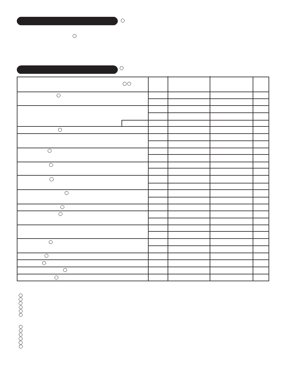
ABSOLUTE MAXIMUM RATINGS
+10V
5A
-55°C to +125°C
-40°C to +85°C
Supply Voltage
Output Current
Case Operating Temperature Range
MSK5921K/H RH
MSK5921RH
-65°C to +150°C
300°C
See SOA Curve
150°C
1
2
3
4
5
6
7
8
9
10
11
12
TST
TLD
PD
TC
+VIN
IOUT
TC
Unless otherwise specified, VIN=5.0V, R1=1.62K, VSHUTDOWN=0V and IOUT=10mA. See Figure 2, typical application circuits.
Guaranteed by design but not tested. Typical parameters are representative of actual device performance but are for reference only.
Industrial grade devices shall be tested to subgroups 1 and 4 unless otherwise requested.
Military grade devices ("H" suffix) shall be 100% tested to subgroups 1,2,3 and 4.
Subgroup 5 and 6 testing available upon request.
Subgroup 1,4
TC=+25°C
Subgroup 2,5
Subgroup 3,6
TA=-55°C
Output current limit is dependent upon the values of VIN and VOUT. See Figure 1 and typical performance curves.
Continuous operation at or above absolute maximum ratings may adversely effect the device performance and/or life cycle.
VIN shall be as specified or VIN Min, whichever is greater.
Not applicable when VOUT<VIN Min - dropout voltage maximum.
Pre and post irradiation limits, up to 100Krad TID, are identical unless otherwise specified.
Reference DSCC SMD 5962R05220 for electrical specifications for devices purchased as such.
NOTES:
○○○○○
○○○○○○○○
○○○○○○
○
○○○○○
○○○○○○
○○○○
○
Group A
Subgroup
1
2,3
1
2,3
1
1,2,3
1
2,3
1
2,3
1
2,3
1
2,3
1
2,3
-
1
2,3
1
2,3
4
5,6
4
-
10mA ≤ IOUT ≤ 1.0A
IOUT=1A R1=187Ω
VFB=1.265V 10mA ≤ IOUT ≤ 3.0A
VIN=6.5V
Not Including IOUT
IOUT=50mA
VOUT+0.4V ≤ VIN ≤ IOUT+1.3V
50mA ≤ IOUT ≤ 3.0A
Delta FB=1% IOUT=2.5A
2.9V ≤ VIN ≤ 6.5V
R1=187Ω
VIN=6.5V
VIN=3.5V VOUT=2.5V
VOUT ≤ 0.2V (OFF)
VOUT=Nominal (ON)
f=120Hz
IOUT =50mA
Referred to Feedback Pin
Junction to Case @ 125°C Output Device
Typ.
-
1.265
-
14
±0.01
-
±0.06
-
0.22
0.26
8
9
-
4.0
1.3
-
70
18
-
2.2
Test Conditions
Max.
6.5
1.305
1.315
5.0
20
±0.50
±2.5
±0.80
±2.5
0.40
10
6.0
5.0
1.6
-
50
4.0
Min.
2.9
1.225
1.215
0
-
1.5
3.0
1.0
65
30
10
-
Min.
2.9
-
1.202
-
0
-
1.5
3.0
-
1.0
-
65
-
30
10
-
Max.
6.5
-
1.328
-
5.0
20
-
±0.60
-
±1.0
-
0.45
-
10
-
6.0
5.0
-
1.6
-
50
4.0
Typ.
-
1.265
-
14
-
0.01
-
0.06
-
0.22
-
8
-
4.0
-
1.3
-
70
18
-
2.2
V
μA
mA
%VOUT
V
mA
V
A
V
dB
degrees
dB
μVRMS
°C/W
MSK5921K/H
MSK5921
Parameter
ELECTRICAL SPECIFICATIONS
2
Units
○
○○○○○○○
1
○○○○○
○○○○○○○○○
○
○○○○○
2
7
2
8
7
10
9
11
Rev. L 1/11
Post Radiation
12
相關PDF資料 |
PDF描述 |
|---|---|
| MSK604B | NEGATIVE OUTPUT WIDE BANDWIDTH HIGH VOLTAGE AMPLIFIER |
| MSK613H | HIGH VOLTAGE/HIGH SPEED SURFACE MOUNT AMPLIFIER |
| MSK641B | WIDE BANDWIDTH, VERY HIGH VOLTAGE CRT VIDEO AMPLIFIER |
| MSK642B | WIDE BANDWIDTH, HIGH VOLTAGE CRT VIDEO AMPLIFIER |
| MSK643B | WIDE BANDWIDTH, VERY HIGH VOLTAGE CRT VIDEO AMPLIFIER |
相關代理商/技術參數(shù) |
參數(shù)描述 |
|---|---|
| MSK600 | 制造商:MSK 制造商全稱:M.S. Kennedy Corporation 功能描述:WIDE BANDWIDTH HIGH VOLTAGE AMPLIFIER |
| MSK601 | 制造商:MSK 制造商全稱:M.S. Kennedy Corporation 功能描述:WIDE BANDWIDTH HIGH VOLTAGE AMPLIFIER |
| MSK601B | 制造商:MSK 制造商全稱:M.S. Kennedy Corporation 功能描述:WIDE BANDWIDTH HIGH VOLTAGE AMPLIFIER |
| MSK604 | 制造商:MSK 制造商全稱:M.S. Kennedy Corporation 功能描述:NEGATIVE OUTPUT WIDE BANDWIDTH HIGH VOLTAGE AMPLIFIER |
| MSK604B | 制造商:MSK 制造商全稱:M.S. Kennedy Corporation 功能描述:NEGATIVE OUTPUT WIDE BANDWIDTH HIGH VOLTAGE AMPLIFIER |
發(fā)布緊急采購,3分鐘左右您將得到回復。