- 您現(xiàn)在的位置:買賣IC網(wǎng) > PDF目錄369930 > MRFIC2403 (MOTOROLA INC) 2.4 GHz POWER AMPLIFIER GaAs MONOLITHIC INTEGRATED CIRCUIT PDF資料下載
參數(shù)資料
| 型號: | MRFIC2403 |
| 廠商: | MOTOROLA INC |
| 元件分類: | 衰減器 |
| 英文描述: | 2.4 GHz POWER AMPLIFIER GaAs MONOLITHIC INTEGRATED CIRCUIT |
| 中文描述: | 2200 MHz - 2700 MHz RF/MICROWAVE NARROW BAND MEDIUM POWER AMPLIFIER |
| 封裝: | LOW PROFILE PLASTIC, SO-16 |
| 文件頁數(shù): | 5/6頁 |
| 文件大?。?/td> | 100K |
| 代理商: | MRFIC2403 |

5
MRFIC2403
MOTOROLA RF DEVICE DATA
TYPICAL CHARACTERISTICS
70
0
PIN, INPUT POWER (dBm)
o
,
o
,
PCNTRL, (VOLTS)
25
5
– 5
5
2
0
f, FREQUENCY (GHz)
26
22
18
3.0
2.8
2.2
2.0
2.6
2.4
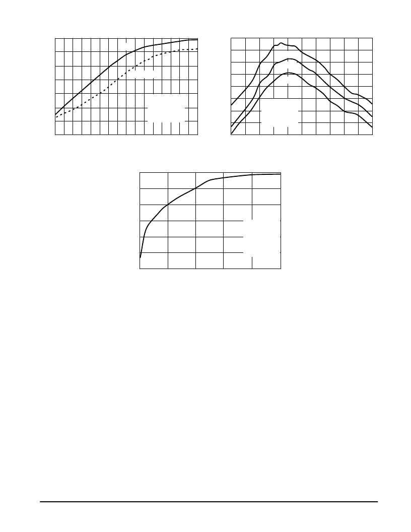
Figure 2. Output Power and Efficiency versus
Input Power
25
21
15
– 6
Figure 3. Output Power versus Frequency
0
Figure 4. Output Power versus PCNTRL Voltage
2.1
2.3
2.5
2.7
2.9
– 8
– 4
– 2
2
4
13
19
20
24
23
25
21
20
0
10
15
1
o
23
19
17
–10
4
6
,
EFFICIENCY
POUT
f = 2.45 GHz
Pin = +4.0 dBm
VDD = 5.0 Vdc
VG1 = –1.0 Vdc
VG2 = –2.0 Vdc
Pin = +4.0 dBm
VDD = 5.0 Vdc
VG1 = –1.0 Vdc
VG2 = –2.0 Vdc
TA = – 30
°
C
25
°
C
85
°
C
3
10
20
30
40
50
60
P
f = 2.45 GHz
VDD = 5.0 Vdc
VG1 = –1.0 Vdc
VG2 = –2.0 Vdc
11
DESIGN AND APPLICATIONS INFORMATION
The MRFIC2403 is a two–stage power amplifier designed
using Motorola’s MAFET planar, refractory gate MESFET IC
process. The RF MESFETs are power, depletion mode
devices and, therefore, require negative bias on the MESFET
gates. For class B operation, –1.0 Vdc is applied to VG1 and
–2.0 Vdc is applied to VG2. Class A biasing will yield slightly
higher gain and 1.0 dB compression point and can be accom-
plished by adjusting the bias on VG1 for IDQ1 = 24 mA and
VG2 for IDQ2 = 96 mA. Where negative voltages are not
already available, Motorola’s MC33128 Power Management
IC can produce –2.5 Vdc from a single positive supply.
The device is capable of better than +23 dBm saturated
output power in the 2.4 to 2.5 GHz ISM band with the output
matching circuit shown in Figure 1. The device can be
operated at other frequencies in the 2.0 GHz to 3.0 GHz
range with this circuit but performance can be improved
with tuning for the specific frequency of use. Input match-
ing is provided on chip. This circuit provides the best gain,
saturated output power and efficiency tradeoff. Saturated
operation has the advantage of best efficiency with less
variation in performance over frequency and temperature.
Operation in saturation is acceptable for constant enve-
lope modulation schemes such as 2 and 4 level FM as spe-
cified for frequency hopping (FHSS) radios in the proposed
IEEE 802.11 PHY layer specification. For direct sequence
(DSSS) IEEE 802.11 operation, where differential binary
phase shift keying (DBPSK) and differential quadrature
phase shift keying (DQPSK) are specified, the amplifier will
have to be “backed off” from saturation by 5.0 dB or more to
avoid spectral regrowth. Care must be taken in the layout of
the circuit and controlled impedance lines must be used at
the RF pins. Capacitive bypassing as shown in the Applica-
tions Circuit must be implemented as close to the chip as
possible to avoid amplifier instability. Additionally, the supply
voltage should be supported by sufficient “stiffening” capaci-
tance, typically electrolytic or tantalum bypass capacitors, to
eliminate noise from digital circuits.
Output power control is accomplished by varying the volt-
age on the PCNTRL pin. 0 Vdc gives minimum output and
reduces the current drawn by the amplifier to the quiescent
value. The amplifier can be put into “sleep” mode by
decreasing the voltage on the gate bias pins to –3.0 Vdc and
the current drain is reduced to a few hundred microamps.
EVALUATION BOARDS
Evaluation boards are available for RF Monolithic Inte-
grated Circuits by adding a “TF” suffix to the device type.
For a complete list of currently available boards and ones
in development for newly introduced poduct, please con-
tact your local Motorola Distributor or Sales Office.
相關(guān)PDF資料 |
PDF描述 |
|---|---|
| MRFIC2404 | 2.4 GHz EXCITER AMPLIFIER GaAs MONOLITHIC INTEGRATED CIRCUIT |
| MRFIC2406 | SOCKET ADAPTER FOR SOIC20 |
| MRFIC2408 | single chip RF Power Amplifier |
| MRFIC2408PP | 28F128/320/640J3A |
| MSC2295-BT1 | NPN RF Amplifier Transistors Surface Mount |
相關(guān)代理商/技術(shù)參數(shù) |
參數(shù)描述 |
|---|---|
| MRFIC2403R2 | 制造商:Freescale Semiconductor 功能描述: |
| MRFIC2404 | 制造商:MOTOROLA 制造商全稱:Motorola, Inc 功能描述:2.4 GHz EXCITER AMPLIFIER GaAs MONOLITHIC INTEGRATED CIRCUIT |
| MRFIC2406 | 制造商:MOTOROLA 制造商全稱:Motorola, Inc 功能描述:2.4 GHz INTEGRATED UPMIXER GaAs MONOLITHIC INTEGRATED CIRCUIT |
| MRFIC2408 | 制造商:MOTOROLA 制造商全稱:Motorola, Inc 功能描述:single chip RF Power Amplifier |
| MRFIC2408PP | 制造商:MOTOROLA 制造商全稱:Motorola, Inc 功能描述:single chip RF Power Amplifier |
發(fā)布緊急采購,3分鐘左右您將得到回復。