- 您現(xiàn)在的位置:買賣IC網(wǎng) > PDF目錄25642 > MR83C154XXX-12/883 (ATMEL CORP) 8-BIT, MROM, 12 MHz, MICROCONTROLLER, CQCC44 PDF資料下載
參數(shù)資料
| 型號: | MR83C154XXX-12/883 |
| 廠商: | ATMEL CORP |
| 元件分類: | 微控制器/微處理器 |
| 英文描述: | 8-BIT, MROM, 12 MHz, MICROCONTROLLER, CQCC44 |
| 封裝: | LCC-44 |
| 文件頁數(shù): | 2/91頁 |
| 文件大小: | 19688K |
| 代理商: | MR83C154XXX-12/883 |
第1頁當前第2頁第3頁第4頁第5頁第6頁第7頁第8頁第9頁第10頁第11頁第12頁第13頁第14頁第15頁第16頁第17頁第18頁第19頁第20頁第21頁第22頁第23頁第24頁第25頁第26頁第27頁第28頁第29頁第30頁第31頁第32頁第33頁第34頁第35頁第36頁第37頁第38頁第39頁第40頁第41頁第42頁第43頁第44頁第45頁第46頁第47頁第48頁第49頁第50頁第51頁第52頁第53頁第54頁第55頁第56頁第57頁第58頁第59頁第60頁第61頁第62頁第63頁第64頁第65頁第66頁第67頁第68頁第69頁第70頁第71頁第72頁第73頁第74頁第75頁第76頁第77頁第78頁第79頁第80頁第81頁第82頁第83頁第84頁第85頁第86頁第87頁第88頁第89頁第90頁第91頁

107
Atmel ATmega16/32/64/M1/C1 [DATASHEET]
7647K–AVR–12/13
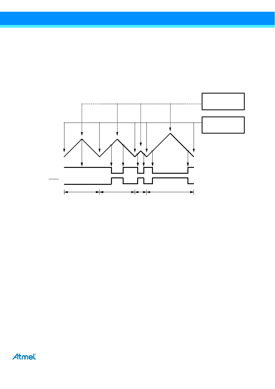
In phase and frequency correct PWM mode the counter is incremented until the counter value matches either the value in ICRn
(WGMn3:0 = 8), or the value in OCRnA (WGMn3:0 = 9). The counter has then reached the TOP and changes the count
direction. The TCNTn value will be equal to TOP for one timer clock cycle. The timing diagram for the phase correct and
frequency correct PWM mode is shown on Figure 13-9. The figure shows phase and frequency correct PWM mode when
OCRnA or ICRn is used to define TOP. The TCNTn value is in the timing diagram shown as a histogram for illustrating the dual-
slope operation. The diagram includes non-inverted and inverted PWM outputs.
The small horizontal line marks on the TCNTn slopes represent compare matches between OCRnx and TCNTn. The OCnx
interrupt flag will be set when a compare match occurs.
Figure 13-9. Phase and Frequency Correct PWM Mode, Timing Diagram
The Timer/Counter overflow flag (TOVn) is set at the same timer clock cycle as the OCRnx registers are updated with the
double buffer value (at BOTTOM). When either OCRnA or ICRn is used for defining the TOP value, the OCnA or ICFn flag is set
when TCNTn has reached TOP. The interrupt flags can then be used to generate an interrupt each time the counter reaches the
TOP or BOTTOM value.
When changing the TOP value the program must ensure that the new TOP value is higher or equal to the value of all of the
compare registers. If the TOP value is lower than any of the compare registers, a compare match will never occur between the
TCNTn and the OCRnx.
As Figure 13-9 shows the output generated is, in contrast to the phase correct mode, symmetrical in all periods. Since the
OCRnx registers are updated at BOTTOM, the length of the rising and the falling slopes will always be equal. This gives
symmetrical output pulses and is therefore frequency correct.
Using the ICRn register for defining TOP works well when using fixed TOP values. By using ICRn, the OCRnA register is free to
be used for generating a PWM output on OCnA. However, if the base PWM frequency is actively changed by changing the TOP
value, using the OCRnA as TOP is clearly a better choice due to its double buffer feature.
In phase and frequency correct PWM mode, the compare units allow generation of PWM waveforms on the OCnx pins. Setting
the COMnx1:0 bits to two will produce a non-inverted PWM and an inverted PWM output can be generated by setting the
COMnx1:0 to three (See Table on page 111). The actual OCnx value will only be visible on the port pin if the data direction for
the port pin is set as output (DDR_OCnx). The PWM waveform is generated by setting (or clearing) the OCnx register at the
compare match between OCRnx and TCNTn when the counter increments, and clearing (or setting) the OCnx register at
compare match between OCRnx and TCNTn when the counter decrements. The PWM frequency for the output when using
phase and frequency correct PWM can be calculated by the following equation:
The N variable represents the prescaler divider (1, 8, 64, 256, or 1024).
1
2
34
TCNTn
(COMnx1:0 = 2)
(COMnx1:0 = 3)
OCnx
Period
OCnA Interrupt Flag Set
or ICFn Interrupt Flag Set
(Interrupt on TOP)
OCRnx/ TOP Update and
TOVn Interrupt Flag Set
(Interrupt on Bottom)
f
OCnxPFCPWM
f
clk_I/O
2 NTOP
----------------------------
=
相關PDF資料 |
PDF描述 |
|---|---|
| MD83C154CXXX-L16P883D | 8-BIT, MROM, 16 MHz, MICROCONTROLLER, CDIP40 |
| MC80C52TXXX-12P883D | 8-BIT, MROM, 12 MHz, MICROCONTROLLER, CDIP40 |
| MQ80C52TXXX-36P883 | 8-BIT, MROM, 36 MHz, MICROCONTROLLER, CQFP44 |
| MQ83C154TXXX-L16/883D | 8-BIT, MROM, 16 MHz, MICROCONTROLLER, CQFP44 |
| MQ80C154-36P883 | 8-BIT, 36 MHz, MICROCONTROLLER, CQFP44 |
相關代理商/技術參數(shù) |
參數(shù)描述 |
|---|---|
| MR850 | 功能描述:整流器 3.0 Amp 50 Volt 150ns RoHS:否 制造商:Vishay Semiconductors 產(chǎn)品:Standard Recovery Rectifiers 配置: 反向電壓:100 V 正向電壓下降: 恢復時間:1.2 us 正向連續(xù)電流:2 A 最大浪涌電流:35 A 反向電流 IR:5 uA 安裝風格:SMD/SMT 封裝 / 箱體:DO-221AC 封裝:Reel |
| MR850 _AY _10001 | 制造商:PanJit Touch Screens 功能描述: |
| MR850 R0 | 制造商:SKMI/Taiwan 功能描述:Diode Switching 50V 3A 2-Pin DO-201AD T/R |
| MR850_ R2 _10001 | 制造商:PanJit Touch Screens 功能描述: |
| MR850_09 | 制造商:PANJIT 制造商全稱:Pan Jit International Inc. 功能描述:SOFT RECOVERY, FAST SWITCHING PLASTIC RECTIFIER |
發(fā)布緊急采購,3分鐘左右您將得到回復。